 ChipApex | Global Electronic Components Supplier
SEARCH
Search Product
Search Post
— IC芯片 | 连接器 | 传感器 | 被动器件 —
Search productSearch post
— IC芯片 | 连接器 | 传感器 | 被动器件 —
Consult the customer manager about the wholesale price.
consultation hotline:86-132-6715-2157
email:[email protected]
Contact the product manager for consultation. One-stop consultation is available.
Do you want a lower wholesale price? Please send us your inquiry and we will reply immediately.
The Infineon BSO612CV is a SIPMOS small-signal transistor featuring dual N- and P-channel enhancement mode MOSFETs in an SO-8 package. The N-channel device supports a maximum drain-source voltage of 60 V, continuous drain current of 3 A, and on-state resistance up to 0.12 Ω. The P-channel counterpart provides -60 V breakdown, -2 A current capability, and resistance up to 0.3 Ω. Both channels are rated for avalanche energy and high dv/dt switching.
Verify the specific ordering code Q67041-S4015 against the datasheet to ensure correct component revision. Confirm that the SO-8 footprint matches the design requirements. Check for any end-of-life notices or alternative recommendations from Infineon, as this is a legacy product series.
Select this component when a matched pair of N- and P-channel logic-level MOSFETs is required in a compact form factor. Ensure the application voltage does not exceed 60 V and current demands fit within the 3 A (N) and 2 A (P) limits. Consider thermal management for power dissipation near the 2 W limit.
Part of the Infineon SIPMOS family designed for small-signal and low-power applications. It integrates complementary transistors to simplify circuit layout for half-bridge or full-bridge topologies. The technology focuses on reliability through avalanche and dv/dt ratings.
Check for direct cross-references with other dual MOSFET packages such as the BSC series or equivalent offerings from other manufacturers. Verify pinout compatibility and electrical parameter margins before substitution.
The N-channel device is rated for 47 mJ and the P-channel for 70 mJ under specified test conditions.
Yes, both channels have a similar threshold voltage range, typically between 2.1 V and 4 V for N-channel and -2.1 V to -4 V for P-channel.
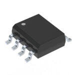 BSO612CV
The activity of extra discounts on wholesale prices is in full swing…
Please fill in your contact information and we will send you the latest wholesale price list.





