 ChipApex | Global Electronic Components Supplier
SEARCH
Search Product
Search Post
— IC芯片 | 连接器 | 传感器 | 被动器件 —
Search productSearch post
— IC芯片 | 连接器 | 传感器 | 被动器件 —
Consult the customer manager about the wholesale price.
consultation hotline:86-132-6715-2157
email:[email protected]
Contact the product manager for consultation. One-stop consultation is available.
Do you want a lower wholesale price? Please send us your inquiry and we will reply immediately.
The UMW BSO615NG is a dual N-channel enhancement mode MOSFET in an SOP-8 package. It features a 60 V drain-source voltage rating and supports up to 7 A continuous drain current at 25 °C case temperature. The device exhibits low on-state resistance, with maximum values of 40 mΩ at VGS = 10 V and 55 mΩ at VGS = 4.5 V. Key dynamic parameters include a total gate charge of 18 nC and a junction-to-ambient thermal resistance of 110 °C/W. Operating temperatures range from -55 °C to +175 °C.
Verify the specific ordering suffix against the manufacturer's official documentation to confirm packaging details such as tape and reel quantities. Ensure that the requested variant matches the required SOP-8 pinout and marking code. Cross-reference the datasheet revision date to confirm parameter validity before finalizing procurement specifications.
Select this component for applications requiring dual channel isolation within a limited footprint. Evaluate the RDS(on) requirements against the intended gate drive voltage, noting the increase at lower VGS levels. Confirm that the thermal management strategy accounts for the specified junction-to-ambient resistance under expected duty cycles.
This part belongs to the UMW SIPMOS series of power MOSFETs designed for general-purpose switching applications. It utilizes trench technology to achieve low on-resistance and fast switching speeds. The dual configuration allows for cost-effective implementation of half-bridge or synchronous rectifier topologies compared to using discrete single devices.
Direct replacements must match the 60 V rating, dual N-channel topology, and SOP-8 package. Verify that substitute parts offer equivalent or superior RDS(on), gate charge, and thermal resistance characteristics to ensure circuit compatibility without redesign.
The maximum single pulse avalanche energy is rated at 16.2 mJ when measured with an inductance of 0.1 mH.
The on-state resistance increases positively with junction temperature. Normalized curves show significant rise at higher temperatures, requiring derating of current capacity accordingly.
The datasheet provides forward voltage characteristics for the source-drain diode but does not explicitly list reverse recovery charge (Qrr) parameters in the static or dynamic tables.
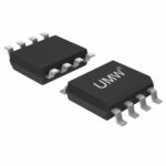 BSO615NG
The activity of extra discounts on wholesale prices is in full swing…
Please fill in your contact information and we will send you the latest wholesale price list.





