ChipApex | Global Electronic Components Supplier
SEARCH
Search Product
Search Post
— IC芯片 | 连接器 | 传感器 | 被动器件 —
Search productSearch post
— IC芯片 | 连接器 | 传感器 | 被动器件 —
Consult the customer manager about the wholesale price.
consultation hotline:86-132-6715-2157
email:[email protected]
Contact the product manager for consultation. One-stop consultation is available.
Do you want a lower wholesale price? Please send us your inquiry and we will reply immediately.
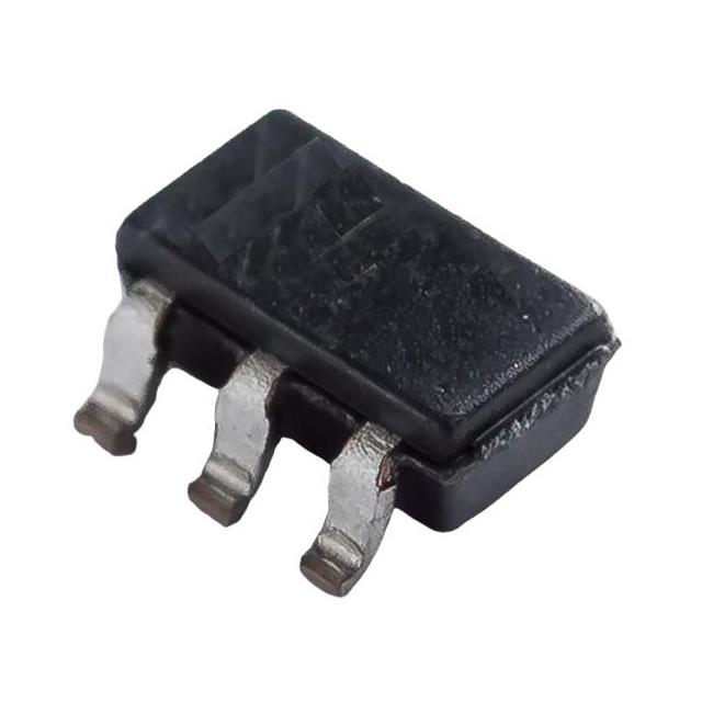
The BSS138DW is a dual N-channel logic level enhancement mode field effect transistor housed in a SOT-363 package. It features a drain-source voltage of 50 V and continuous drain current of 200 mA. The device exhibits a maximum on-state resistance of 3.5 Ω at VGS=10 V and a gate threshold voltage ranging from 0.5 V to 1.6 V. Electrical characteristics include an input capacitance of 50 pF, forward transfer admittance of 100 mS, and switching delay times of 20 ns for both turn-on and turn-off operations.
Verify the specific ordering suffix when purchasing. A blank suffix indicates a lead-free package, while the letter 'G' denotes a halogen-free variant. Confirm that the component matches the SOT-363 footprint dimensions provided in the datasheet to ensure compatibility with existing PCB layouts and soldering profiles.
Select this component for designs requiring dual N-channel MOSFETs in a minimal footprint. The 50 V rating and 200 mA current capacity suit low-power signal switching tasks. Ensure the driving circuit can provide sufficient gate voltage to achieve the specified low on-resistance values during operation.
This part belongs to the family of small-signal N-channel MOSFETs designed for general-purpose switching. It utilizes silicon technology and is qualified for high-reliability applications. The device is manufactured using processes compliant with environmental standards, offering options for lead-free and halogen-free configurations.
Direct substitutes must match the dual N-channel topology and SOT-363 package. Verify that alternative components meet or exceed the 50 V breakdown voltage and 200 mA current ratings. Check pinout compatibility to prevent circuit damage during installation.
 BSS138DW
The activity of extra discounts on wholesale prices is in full swing…
Please fill in your contact information and we will send you the latest wholesale price list.