 ChipApex | Global Electronic Components Supplier

SEARCH
Search Product
Search Post
— IC芯片 | 连接器 | 传感器 | 被动器件 —
Search productSearch post
— IC芯片 | 连接器 | 传感器 | 被动器件 —
Consult the customer manager about the wholesale price.
consultation hotline:86-132-6715-2157
email:[email protected]
Contact the product manager for consultation. One-stop consultation is available.
Do you want a lower wholesale price? Please send us your inquiry and we will reply immediately.
The BSS138K is an N-Channel Logic Level Enhancement Mode Field Effect Transistor manufactured by onsemi. It features a Drain-Source Voltage (VDSS) of 50 V and a continuous Drain Current (ID) of 0.22 A. The device operates within a junction temperature range of -55°C to +150°C with a total power dissipation of 350 mW. Key electrical parameters include a maximum static Drain-Source On-Resistance (RDS(on)) of 2.5 Ω at VGS = 1.8 V, a Gate Threshold Voltage (VGS(th)) ranging from 0.6 V to 1.2 V, and a typical Total Gate Charge (Qg) of 2.4 nC. The component utilizes a SOT-23-3 surface mount package.
Verify the specific ordering suffix against official documentation to confirm packaging details such as tape and reel specifications. Ensure compliance requirements including RoHS status and lead-free designation are validated prior to integration. Cross-reference the manufacturer part number with authorized distribution channels to guarantee authenticity and traceability of the semiconductor components.
Select this component when a small surface-mount footprint is required alongside logic-level gate drive compatibility. Evaluate the thermal resistance and power dissipation limits relative to the expected ambient operating conditions. Confirm that the drain-source breakdown voltage and continuous current ratings exceed the maximum circuit demands to ensure reliable long-term performance.
This device belongs to the BSS138K series of N-channel MOSFETs designed for general-purpose switching applications. Manufactured using silicon technology, it offers a compact SOT-23-3 package suitable for automated surface mount assembly. The product line emphasizes low input leakage and fast switching capabilities for modern electronic designs.
Consult official substitution guides or datasheets for verified equivalent part numbers from onsemi or other manufacturers before implementation.
The maximum Drain-Source Voltage (VDSS) is rated at 50 V.
The Gate Threshold Voltage Temperature Coefficient is approximately -1.4 mV/°C.
The typical Turn-On Delay Time (tD(ON)) is 5 ns under specified test conditions.
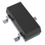 BSS138K

The activity of extra discounts on wholesale prices is in full swing…
Please fill in your contact information and we will send you the latest wholesale price list.





