 ChipApex | Global Electronic Components Supplier

SEARCH
Search Product
Search Post
— IC芯片 | 连接器 | 传感器 | 被动器件 —
Search productSearch post
— IC芯片 | 连接器 | 传感器 | 被动器件 —
Consult the customer manager about the wholesale price.
consultation hotline:86-132-6715-2157
email:[email protected]
Contact the product manager for consultation. One-stop consultation is available.
Do you want a lower wholesale price? Please send us your inquiry and we will reply immediately.
The BSS209PW is a P-Channel enhancement mode small-signal MOSFET from Infineon Technologies, utilizing OptiMOS-P technology. It features a -20 V drain-source breakdown voltage and a continuous drain current of -0.58 A at 25°C. The device operates within a temperature range of -55°C to +150°C and is housed in an SOT-323 package. Key electrical characteristics include a maximum on-state resistance of 550 mΩ at VGS = -4.5V and a gate threshold voltage ranging from -0.6 V to -1.2 V. It supports avalanche energy ratings up to 3.5 mJ and reverse diode dv/dt ratings of -6 kV/µs.
Verify the specific ordering code Q67042-S4074 against procurement requirements. Confirm that the component meets IEC climatic category standards (55/150/56) for intended environmental conditions. Ensure design compliance with the specified thermal resistance values for both junction-to-soldering point and junction-to-ambient scenarios.
Select this component for designs requiring a compact P-Channel solution with logic-level gate drive compatibility. The SOT-323 package suits space-constrained PCB layouts. Consider the 550 mΩ maximum RDS(on) for low-current switching efficiency. Verify that the -20 V rating aligns with system voltage levels to prevent breakdown under operating conditions.
This part belongs to Infineon's OptiMOS-P small-signal transistor portfolio. It is designed for general-purpose switching and amplification tasks where low cost and small footprint are prioritized. The device is manufactured using silicon technology and is compliant with RoHS directives.
No officially confirmed substitute part numbers are documented in the provided datasheet.
The single pulse avalanche energy rating is 3.5 mJ when ID is -0.58 A, VDD is -10 V, and RGS is 25 Ω.
Yes, the BSS209PW is dv/dt rated with a capability of -6 kV/µs under specified test conditions.
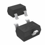 BSS209PW

The activity of extra discounts on wholesale prices is in full swing…
Please fill in your contact information and we will send you the latest wholesale price list.





