 ChipApex | Global Electronic Components Supplier
SEARCH
Search Product
Search Post
— IC芯片 | 连接器 | 传感器 | 被动器件 —
Search productSearch post
— IC芯片 | 连接器 | 传感器 | 被动器件 —
Consult the customer manager about the wholesale price.
consultation hotline:86-132-6715-2157
email:[email protected]
Contact the product manager for consultation. One-stop consultation is available.
Do you want a lower wholesale price? Please send us your inquiry and we will reply immediately.
The BSS8402DW-7-F is a complementary pair enhancement mode MOSFET in an SOT363 package. It integrates an N-channel device (Q1) and a P-channel device (Q2). Q1 features a 60V drain-source voltage, 115mA continuous current, and 13.5Ω on-resistance at VGS=10V. Q2 provides -50V breakdown, -130mA current, and 10Ω on-resistance at VGS=-5V. The total power dissipation is 200mW with a thermal resistance of 625°C/W. Operating temperature ranges from -55°C to +150°C.
Verify the specific ordering suffix to confirm packaging quantity. The -7-F suffix indicates a 3,000-unit tape and reel format. Ensure compatibility with standard surface mount assembly processes. Confirm that the standard grade meets project requirements rather than the automotive qualified variant.
Select this component when a matched N-P channel pair is required in a minimal footprint. The SOT363 case size supports high-density board layouts. Consider the distinct drive voltages; Q1 requires 10V for optimal RDS(ON), while Q2 operates effectively at -5V. Verify thermal constraints given the 625°C/W junction-to-ambient resistance.
This part belongs to Diodes Incorporated's complementary MOSFET family, specifically combining a 2N7002-type N-channel structure with a BSS84-type P-channel structure. It serves as a compact solution for dual-transistor circuits where matching characteristics and small physical dimensions are prioritized over high-power handling capabilities.
Public confirmed substitute: BSS8402DWQ-7-F. This variant offers AEC-Q101 qualification and IATF 16949 manufacturing certification while maintaining identical electrical specifications and packaging.
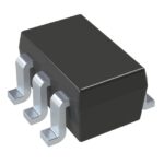 BSS8402DW-7-F
The activity of extra discounts on wholesale prices is in full swing…
Please fill in your contact information and we will send you the latest wholesale price list.





