 ChipApex | Global Electronic Components Supplier
SEARCH
Search Product
Search Post
— IC芯片 | 连接器 | 传感器 | 被动器件 —
Search productSearch post
— IC芯片 | 连接器 | 传感器 | 被动器件 —
Consult the customer manager about the wholesale price.
consultation hotline:86-132-6715-2157
email:[email protected]
Contact the product manager for consultation. One-stop consultation is available.
Do you want a lower wholesale price? Please send us your inquiry and we will reply immediately.
The BSS8402DW-7-G is a complementary pair enhancement mode MOSFET in an SOT363 package. It integrates an N-channel device (Q1) and a P-channel device (Q2). Q1 features a drain-source breakdown voltage of 60V, continuous drain current of 115mA at +25°C, and on-resistance of 13.5Ω max at VGS=10V. Q2 has a breakdown voltage of -50V, continuous drain current of -130mA, and on-resistance of 10Ω max at VGS=-5V. The total power dissipation is 200mW with a thermal resistance of 625°C/W. Operating temperature range spans from -55°C to +150°C.
Verify the specific ordering suffix against official Diodes Incorporated documentation to confirm packaging quantity and compliance status. The datasheet lists standard tape and reel options such as -7-F and -13-F. Confirm that the -G suffix aligns with the required manufacturing specifications and environmental declarations before finalizing procurement orders.
Select this component when a compact dual-transistor solution is required for low-voltage signal switching or logic level translation. The SOT363 package minimizes board space compared to discrete single transistors. Ensure the application voltage does not exceed 60V for the N-channel section or 50V for the P-channel section while considering the 200mW total power dissipation limit.
This part belongs to the BSS8402DW family of complementary MOSFET pairs manufactured by Diodes Incorporated. It serves as a monolithic alternative to using separate N-channel and P-channel devices, simplifying circuit design for general-purpose switching tasks. The device utilizes molded plastic case material with a UL 94V-0 flammability rating.
Direct replacements include the BSS8402DW-7-F and BSS8402DW-13-F variants which share identical electrical characteristics but differ in reel packaging quantities.
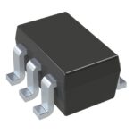 BSS8402DW-7-G
The activity of extra discounts on wholesale prices is in full swing…
Please fill in your contact information and we will send you the latest wholesale price list.





