 ChipApex | Global Electronic Components Supplier
SEARCH
Search Product
Search Post
— IC芯片 | 连接器 | 传感器 | 被动器件 —
Search productSearch post
— IC芯片 | 连接器 | 传感器 | 被动器件 —
Consult the customer manager about the wholesale price.
consultation hotline:86-132-6715-2157
email:[email protected]
Contact the product manager for consultation. One-stop consultation is available.
Do you want a lower wholesale price? Please send us your inquiry and we will reply immediately.
The BSS84V-7 is a dual P-channel enhancement mode field effect transistor manufactured by Diodes Incorporated. It integrates two independent P-channel MOSFETs within a single surface-mount package, designed for low-power switching applications. The device operates with a maximum drain-source voltage of 50 V and supports a continuous drain current of 130 mA per channel. Key electrical characteristics include a gate-source voltage rating of ±20 V and a maximum power dissipation of 300 mW at 25°C ambient temperature. The component functions reliably across an operating temperature range from -55°C to +150°C junction temperature.
Verify the specific datasheet revision (DS30605 Rev. 7) when sourcing, as manufacturing updates may occur. Confirm package marking codes match the official Diodes Incorporated specifications. Ensure compliance with RoHS directives if required for your assembly process. Cross-reference pinouts carefully against the SOT-363 or SC-88 footprint depending on the exact variant supplied.
Select this component when space constraints require dual switching functionality in a minimal footprint. Compare Rds(on) values at specific Vgs levels against alternative dual P-channel MOSFETs to ensure compatibility with your logic drive voltages. Verify that the 130 mA current rating meets the peak load requirements of your application without exceeding thermal limits.
This part belongs to the BSS84 family of dual P-channel MOSFETs from Diodes Incorporated. It shares functional similarities with parts like the BSS84DW-7-F but may differ in specific packaging dimensions or internal die configurations. The 'V' suffix typically denotes a specific package style or revision within the manufacturer's lineup, distinct from single-channel variants like the BSS84-7.
Direct substitutes include the BSS84DW-7-F from Diodes Incorporated. Other compatible dual P-channel MOSFETs from manufacturers such as Alpha & Omega Semiconductor (e.g., AO4801, AO4813) may serve as alternatives if pinout and electrical parameters align with the design requirements.
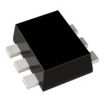 BSS84V-7
The activity of extra discounts on wholesale prices is in full swing…
Please fill in your contact information and we will send you the latest wholesale price list.





