ChipApex | Global Electronic Components Supplier
SEARCH
Search Product
Search Post
— IC芯片 | 连接器 | 传感器 | 被动器件 —
Search productSearch post
— IC芯片 | 连接器 | 传感器 | 被动器件 —
Consult the customer manager about the wholesale price.
consultation hotline:86-132-6715-2157
email:[email protected]
Contact the product manager for consultation. One-stop consultation is available.
Do you want a lower wholesale price? Please send us your inquiry and we will reply immediately.
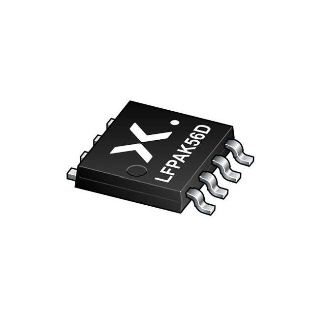
The Nexperia BUK9V13-40HX is a dual N-channel logic level MOSFET in an LFPAK56D (SOT1205) package, configured as a half-bridge switch. It utilizes Trench 9 technology and is qualified to AEC-Q101 standards. Key electrical parameters include a drain-source voltage of 40 V, continuous drain current of 42 A at 25 °C, and a maximum on-state resistance of 13.6 mΩ at VGS = 10 V. The device features a total gate charge of 13.9 nC, thermal resistance from junction to mounting base of 3 K/W, and operates within a temperature range of -55 °C to +175 °C.
Verify the specific ordering suffix 'X' against the manufacturer's official documentation to confirm reel specifications and tape-and-reel dimensions. Ensure the component matches the SOT1205 package outline and that the marking code corresponds to the intended part number. Confirm compliance requirements such as REACH and RoHS status directly from the latest datasheet before finalizing procurement.
Select this component for designs requiring a pre-configured half-bridge topology to reduce footprint and parasitic inductance. The logic level gate drive capability supports direct interfacing with standard microcontrollers. Consider the 175 °C junction temperature rating for thermally demanding environments. Verify that the PCB thermal design can handle the specified power dissipation limits under actual operating conditions.
This device belongs to Nexperia's portfolio of automotive-qualified power switches utilizing Trench 9 superjunction technology. It is designed specifically for high-performance PWM applications where space constraints and efficiency are critical. The LFPAK56D package variant offers footprint compatibility with other dual packages while providing enhanced thermal performance through its copper clip construction.
Direct substitutes must match the LFPAK56D (SOT1205) package, 40 V rating, and half-bridge configuration. Verify that alternative parts meet AEC-Q101 qualification if automotive use is required. Check pinout compatibility, specifically the shared S1/D2 node, to ensure seamless integration without PCB redesign.
An internal connection links the source of the high-side FET (S1) to the drain of the low-side FET (D2), creating a common midpoint suitable for half-bridge switching applications.
The device is rated for a maximum junction temperature of 175 °C, making it suitable for thermally demanding automotive environments.
Yes, it is a logic level MOSFET designed to be fully enhanced with standard logic voltages, such as 4.5 V or 10 V gate-source drive.
 BUK9V13-40HX
The activity of extra discounts on wholesale prices is in full swing…
Please fill in your contact information and we will send you the latest wholesale price list.