ChipApex | Global Electronic Components Supplier
SEARCH
Search Product
Search Post
— IC芯片 | 连接器 | 传感器 | 被动器件 —
Search productSearch post
— IC芯片 | 连接器 | 传感器 | 被动器件 —
Consult the customer manager about the wholesale price.
consultation hotline:86-132-6715-2157
email:[email protected]
Contact the product manager for consultation. One-stop consultation is available.
Do you want a lower wholesale price? Please send us your inquiry and we will reply immediately.
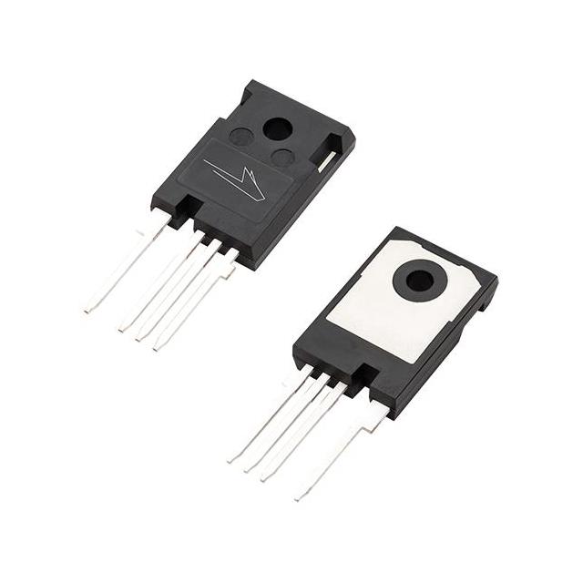
The C3M0021120K is a third-generation Silicon Carbide (SiC) N-Channel Enhancement Mode MOSFET manufactured by Wolfspeed. It features a TO-247-4L package with a separate driver source pin and an 8mm creepage distance between drain and source. Key electrical parameters include a 1200V drain-source voltage, a maximum on-resistance of 28.8mΩ at 50A and 15V, and a continuous drain current of 100A at 25°C case temperature. The device supports a junction temperature range from -40°C to +175°C.
Verify the specific revision level against the manufacturer's datasheet before procurement, as technical specifications may be subject to change without notice. Confirm that the TO-247-4L package dimensions and solder pad layouts match the target PCB design requirements. Ensure compliance with relevant environmental directives such as RoHS and REACH based on the latest product documentation provided by Wolfspeed.
Select this component for designs requiring high blocking voltage combined with low on-resistance to improve system efficiency. The separate driver source pin facilitates easier layout for reducing parasitic inductance and gate ringing. Consider the thermal resistance characteristics when designing heat dissipation solutions to maintain the junction temperature within the specified operating range during high-current operation.
This part belongs to the C3M™ family of discrete Silicon Carbide Power MOSFETs from Wolfspeed. The family utilizes industry-standard packages to allow flexible system upgrades and cost optimization. The C3M0021120K specifically targets applications demanding high power density and increased switching frequencies compared to traditional silicon-based technologies.
Direct replacements within the same series include C3M0016120K and C3M0032120K, which share the TO-247-4L package but offer different on-resistance and current ratings. Verify compatibility with existing gate drive circuits and thermal management systems when substituting these variants.
The fourth pin serves as a separate driver source connection. This design helps reduce switching losses and minimizes gate ringing by isolating the high-current source path from the sensitive gate drive return path.
The internal gate resistance is approximately 3.3 Ω. External gate resistors can be used in conjunction with this internal resistance to tune switching speeds and manage electromagnetic interference (EMI), balancing switching losses against voltage overshoot.
 C3M0021120K
The activity of extra discounts on wholesale prices is in full swing…
Please fill in your contact information and we will send you the latest wholesale price list.