ChipApex | Global Electronic Components Supplier
SEARCH
Search Product
Search Post
— IC芯片 | 连接器 | 传感器 | 被动器件 —
Search productSearch post
— IC芯片 | 连接器 | 传感器 | 被动器件 —
Consult the customer manager about the wholesale price.
consultation hotline:86-132-6715-2157
email:[email protected]
Contact the product manager for consultation. One-stop consultation is available.
Do you want a lower wholesale price? Please send us your inquiry and we will reply immediately.
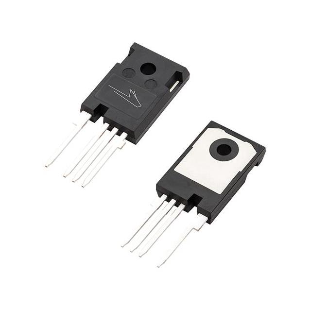
The Wolfspeed C3M0025065K is a third-generation silicon carbide (SiC) MOSFET featuring N-channel enhancement mode technology. It provides a drain-source voltage of 650 V and a typical on-resistance of 25 mΩ at 25°C. The device supports a continuous drain current of 97 A and a pulsed drain current of 251 A. Key electrical parameters include a total gate charge of 112 nC, an input capacitance of 2980 pF, and a reverse recovery charge of 453 nC for the intrinsic diode. It operates within a junction temperature range of -40°C to +175°C.
Verify component authenticity through authorized distributors or Wolfspeed directly. Confirm datasheet revision status, specifically Rev. 03 from September 2024, as specifications may evolve. Ensure compliance with RoHS and REACH requirements by requesting current declarations. Validate package integrity upon receipt, checking for physical damage to the TO-247-4L leads. Cross-reference ordering suffixes to confirm exact configuration matches design requirements.
Select this component for designs requiring high efficiency and power density in 650 V applications. The TO-247-4L package facilitates easy paralleling and simple driving due to the Kelvin source connection. Consider thermal management capabilities, noting the low thermal resistance from junction to case. Evaluate system switching frequency requirements against the device's low capacitance profile. Ensure gate drive voltages align with the recommended operational limits for optimal performance.
This part belongs to the Wolfspeed C3M series of discrete silicon carbide power MOSFETs. It represents an advancement over previous generations, offering improved switching speeds and reduced losses. The product line targets high-performance power conversion systems where size, weight, and efficiency are critical constraints. It complements other Wolfspeed SiC devices like Schottky diodes for complete solution development.
Direct substitutes within the same family include C3M0015065K and C3M0045065K, which share similar packaging but differ in on-resistance ratings. Verify pinout compatibility and thermal characteristics when considering alternatives. Ensure any replacement maintains the required 650 V blocking voltage and meets the specific current handling needs of the application.
The fourth pin serves as a Kelvin source connection, providing a dedicated path for the gate driver return. This minimizes the impact of stray inductance in the main source path, enabling faster and more stable switching performance.
The device features a fast intrinsic diode with low reverse recovery charge (Qrr). At 25°C, the typical Qrr is 453 nC, which helps reduce switching losses and electromagnetic interference in hard-switching topologies.
 C3M0025065K
The activity of extra discounts on wholesale prices is in full swing…
Please fill in your contact information and we will send you the latest wholesale price list.