ChipApex | Global Electronic Components Supplier
SEARCH
Search Product
Search Post
— IC芯片 | 连接器 | 传感器 | 被动器件 —
Search productSearch post
— IC芯片 | 连接器 | 传感器 | 被动器件 —
Consult the customer manager about the wholesale price.
consultation hotline:86-132-6715-2157
email:[email protected]
Contact the product manager for consultation. One-stop consultation is available.
Do you want a lower wholesale price? Please send us your inquiry and we will reply immediately.
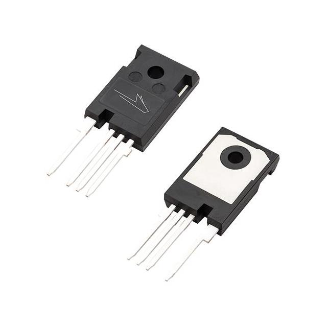
The Wolfspeed C3M0120100K is a Silicon Carbide (SiC) Power MOSFET utilizing C3M technology. It features an N-Channel Enhancement Mode configuration housed in a TO-247-4L package. Key electrical parameters include a Drain-Source Voltage (VDS) of 1000 V, a maximum Gate-Source Voltage (VGS(max)) of +19 V transient and -8 V to +15 V static, and a typical On-State Resistance (RDS(on)) of 120 mΩ at VGS = 15 V and ID = 15 A. The device supports a DC Continuous Drain Current (ID) of 22 A at TC = 25°C and a Pulsed Drain Current (IDM) of 50 A. Thermal characteristics specify a Junction-to-Case thermal resistance (RθJC) of 1.5 °C/W and an operating junction temperature range from -55°C to +150°C.
Verify the specific revision level against the latest official datasheet before finalizing designs, as Wolfspeed periodically updates documentation. Confirm that the TO-247-4L package dimensions align with your PCB footprint requirements. Ensure sourcing channels provide genuine components to guarantee compliance with RoHS and REACh standards. Cross-reference the part number with current manufacturer availability lists to confirm production status.
Select this component for high-voltage applications requiring robust switching performance and low conduction losses. The separate driver source pin facilitates precise gate control, making it suitable for topologies sensitive to parasitic inductance. Evaluate the thermal management strategy based on the specified RθJC and power dissipation limits. Consider the device's high-speed switching capabilities when designing snubber circuits or selecting external gate resistors to optimize EMI and efficiency trade-offs.
This device belongs to the C3M family of Silicon Carbide MOSFETs manufactured by Wolfspeed. The C3M series represents third-generation SiC technology designed for high-power density and efficiency. The TO-247-4L package is an industry-standard form factor widely used in power electronics. This specific model targets applications demanding 1000V blocking capability with optimized switching characteristics.
Direct replacement requires verifying pinout compatibility and electrical parameter equivalence. Check if alternative packages like TO-247-3 are acceptable, noting the absence of the dedicated driver source pin in those variants. Ensure any substitute maintains similar RDS(on), Qrr, and thermal resistance values to preserve system performance and reliability without redesigning the cooling infrastructure.
The separate driver source pin (Pin 3) isolates the high-current power source path from the low-current gate drive return path. This separation minimizes ground bounce and reduces gate ringing during fast switching transitions.
The intrinsic body diode exhibits low reverse recovery charge (Qrr) and fast reverse recovery time (trr). This characteristic reduces switching losses and electromagnetic interference when the diode conducts during dead-time intervals in bridge configurations.
 C3M0120100K
The activity of extra discounts on wholesale prices is in full swing…
Please fill in your contact information and we will send you the latest wholesale price list.