 ChipApex | Global Electronic Components Supplier
SEARCH
Search Product
Search Post
— IC芯片 | 连接器 | 传感器 | 被动器件 —
Search productSearch post
— IC芯片 | 连接器 | 传感器 | 被动器件 —
Consult the customer manager about the wholesale price.
consultation hotline:86-132-6715-2157
email:[email protected]
Contact the product manager for consultation. One-stop consultation is available.
Do you want a lower wholesale price? Please send us your inquiry and we will reply immediately.
The CMLDM3757 TR PBFREE is a surface-mount complementary MOSFET containing N-Channel and P-Channel enhancement-mode devices in an SOT-563 package. The N-Channel transistor supports a continuous drain current of 540 mA with a maximum drain-source voltage of 20 V, while the P-Channel device handles 430 mA at the same voltage rating. Both transistors share a gate-source breakdown voltage of 8.0 V and a total power dissipation capacity of 350 mW under standard thermal conditions. The component operates within a junction temperature range of -65°C to +150°C.
Verify that the ordering suffix PBFREE corresponds to lead-free plating specifications as defined by the manufacturer's standard terms. Confirm the specific marking code 3C7 matches the physical component received. Ensure the procurement documentation references the correct SOT-563 case outline R6 for mechanical compatibility during assembly planning.
Select this component when a compact complementary pair is required for high-speed pulsed amplifier or driver stages. Evaluate the rDS(ON) values at the intended gate drive voltage to ensure adequate efficiency. Consider the 350 mW power dissipation limit and the associated thermal resistance values relative to the target PCB copper pad area for the specific application environment.
This part belongs to Central Semiconductor’s lineup of surface-mount silicon MOSFETs designed for space-constrained designs. It integrates two distinct transistors into one SOT-563 footprint, reducing board space compared to discrete implementations. The complementary configuration simplifies circuit design for push-pull or half-bridge applications requiring matched switching characteristics.
Publicly confirmed substitute part numbers are not available in the provided documentation. Verify pinout compatibility and electrical parameters against potential alternatives before implementation.
The component provides ESD protection up to 1800V based on the Human Body Model.
Maximum power dissipation varies from 150 mW to 350 mW depending on the FR-4 epoxy PC board copper mounting pad area, ranging from 1.4 mm² to 4.0 mm².
The total gate charge (Qg) for the N-Channel is typically 1.58 nC when tested at VDS=10V, VGS=4.5V, and ID=500mA.
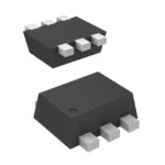 CMLDM3757 TR PBFREE
The activity of extra discounts on wholesale prices is in full swing…
Please fill in your contact information and we will send you the latest wholesale price list.





