 ChipApex | Global Electronic Components Supplier
SEARCH
Search Product
Search Post
— IC芯片 | 连接器 | 传感器 | 被动器件 —
Search productSearch post
— IC芯片 | 连接器 | 传感器 | 被动器件 —
Consult the customer manager about the wholesale price.
consultation hotline:86-132-6715-2157
email:[email protected]
Contact the product manager for consultation. One-stop consultation is available.
Do you want a lower wholesale price? Please send us your inquiry and we will reply immediately.
The CMPF4391 TR TIN/LEAD is a surface-mount N-channel silicon JFET manufactured by Central Semiconductor Corp. It utilizes an epitaxial planar process and is housed in a SOT-23 package with three pins. The device supports a maximum drain-source voltage (VDS) of 40 V and a power dissipation (PD) of 350 mW at 25°C ambient temperature. Electrical characteristics include a drain-source current (IDSS) range of 50 to 150 mA at VDS=20V, a gate-source breakdown voltage (BVGSS) of 40 V, and an input capacitance (Ciss) of up to 14 pF. The component operates within a junction temperature range of -65°C to +150°C.
Verify the specific ordering suffix required for your manufacturing needs. The datasheet indicates that adding the suffix "TIN/LEAD" specifies tin/lead plating, while "PBFREE" denotes lead-free plating. Absence of a suffix may result in either plating type depending on availability. Confirm the reel size (7-inch or 13-inch) corresponds to the "TR" or "TR13" designation in the part number to ensure correct packaging quantities.
Select this component when a single N-channel JFET with a 40 V rating is required in a compact SOT-23 footprint. Ensure the IDSS range of 50–150 mA aligns with the circuit's biasing requirements. Consider the thermal resistance of 357 °C/W and the 350 mW power dissipation limit when designing for thermal management in enclosed environments.
This part belongs to the CMPF4391 series, which includes related devices CMPF4392 and CMPF4393. These components share the same physical package and general electrical ratings but differ in their specific transfer characteristics, such as IDSS ranges and VGS(OFF) values. The CMPF4391 specifically targets applications requiring the higher current and voltage thresholds defined in its datasheet parameters.
Direct substitutes within the same series include CMPF4392 and CMPF4393, though they exhibit different IDSS and VGS(OFF) specifications. Verify pinout compatibility, as all devices in the series use the standard SOT-23 lead configuration: Drain (Pin 1), Source (Pin 2), and Gate (Pin 3). Cross-referencing with other manufacturers' JFETs requires careful validation of electrical limits and package dimensions.
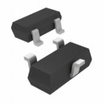 CMPF4391 TR TIN/LEAD
The activity of extra discounts on wholesale prices is in full swing…
Please fill in your contact information and we will send you the latest wholesale price list.






