ChipApex | Global Electronic Components Supplier
SEARCH
Search Product
Search Post
— IC芯片 | 连接器 | 传感器 | 被动器件 —
Search productSearch post
— IC芯片 | 连接器 | 传感器 | 被动器件 —
Consult the customer manager about the wholesale price.
consultation hotline:86-132-6715-2157
email:[email protected]
Contact the product manager for consultation. One-stop consultation is available.
Do you want a lower wholesale price? Please send us your inquiry and we will reply immediately.
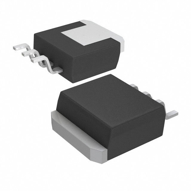
The CSD18510KTT is a single N-channel NexFET power MOSFET manufactured by Texas Instruments. It utilizes silicon technology and features a D2PAK-3 (TO-263-3) surface-mount package. Key electrical specifications include a drain-source breakdown voltage (Vds) of 40 V, a continuous drain current (Id) of 200 A, and a maximum on-resistance (Rds On) of 2 mOhms. The device operates with a gate-source voltage range of -20 V to +20 V and has a gate charge (Qg) of 153 nC. It supports an enhancement mode configuration with rise and fall times of 8 ns. The component is rated for a power dissipation (Pd) of 250 W and functions within a temperature range of -55 °C to +175 °C.
Verify the specific ordering suffix and packaging type against the manufacturer's official datasheet to ensure compatibility with automated assembly processes. Confirm RoHS compliance status and REACH SVHC declarations prior to integration into final products. Ensure that the selected package variant matches the intended PCB footprint and thermal management requirements.
Select this component based on the required 40 V voltage rating and 200 A current handling capacity. Evaluate the 2 mOhm on-resistance against system efficiency targets and thermal constraints. Consider the D2PAK-3 package dimensions for board space limitations and verify that the gate charge characteristics align with the driving circuit's capabilities for optimal switching performance.
This part belongs to the CSD18510 series of NexFET power MOSFETs from Texas Instruments. These devices are engineered to provide superior performance compared to traditional planar MOSFETs, offering lower on-resistance and faster switching speeds. The series is widely used in modern power electronics where efficiency and size reduction are critical design parameters.
Consult the official Texas Instruments substitution guide or cross-reference tools for verified equivalent parts. Ensure any substitute maintains identical pinout, voltage ratings, and thermal characteristics to avoid redesigning the PCB layout or thermal interface.
 CSD18510KTT
The activity of extra discounts on wholesale prices is in full swing…
Please fill in your contact information and we will send you the latest wholesale price list.