 ChipApex | Global Electronic Components Supplier
SEARCH
Search Product
Search Post
— IC芯片 | 连接器 | 传感器 | 被动器件 —
Search productSearch post
— IC芯片 | 连接器 | 传感器 | 被动器件 —
Consult the customer manager about the wholesale price.
consultation hotline:86-132-6715-2157
email:[email protected]
Contact the product manager for consultation. One-stop consultation is available.
Do you want a lower wholesale price? Please send us your inquiry and we will reply immediately.
The CSD25202W15 is a single P-channel power MOSFET from Texas Instruments' NexFET family, manufactured using silicon technology. It features a 20 V drain-source breakdown voltage and supports a continuous drain current of 4 A at ambient temperature. The device offers a maximum on-resistance of 52 mΩ and operates with a gate-source voltage range of ±6 V. Key electrical parameters include a gate charge of 5.8 nC, an input capacitance of 1010 pF, and a threshold voltage of 750 mV. It is housed in a compact 9-DSBGA package, dissipates up to 500 mW, and functions within a junction temperature range of -55°C to +150°C.
Verify the specific ordering suffix (e.g., T) against the manufacturer's datasheet to ensure correct packaging configuration such as reel or cut tape. Confirm RoHS compliance status and moisture sensitivity level requirements prior to procurement. Cross-reference the full part number with official distributor catalogs to validate availability and authenticity.
Select this component for designs requiring a 20 V P-channel switch with moderate current handling capabilities. Ensure the driving circuit can provide sufficient gate voltage swing relative to the source terminal. Evaluate thermal performance based on the 500 mW power dissipation limit and the thermal characteristics of the 9-DSBGA package under expected operating conditions.
This device belongs to the CSD25202W15 series of NexFET power MOSFETs. It represents a single-channel enhancement-mode transistor designed for general-purpose power switching. The product line focuses on balancing low on-resistance with small physical size for portable and space-constrained electronics.
Consult the manufacturer's official substitution guide for verified alternatives. Do not assume functional compatibility with other P-channel MOSFETs without verifying pinout, voltage ratings, and thermal specifications.
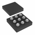 CSD25202W15
The activity of extra discounts on wholesale prices is in full swing…
Please fill in your contact information and we will send you the latest wholesale price list.





