 ChipApex | Global Electronic Components Supplier
SEARCH
Search Product
Search Post
— IC芯片 | 连接器 | 传感器 | 被动器件 —
Search productSearch post
— IC芯片 | 连接器 | 传感器 | 被动器件 —
Consult the customer manager about the wholesale price.
consultation hotline:86-132-6715-2157
email:[email protected]
Contact the product manager for consultation. One-stop consultation is available.
Do you want a lower wholesale price? Please send us your inquiry and we will reply immediately.
The CSD75204W15 is a dual P-channel NexFET power MOSFET in a 1.5-mm × 1.5-mm wafer level package. It features a drain-to-drain voltage of -20 V and a continuous drain current of -3 A at 25°C case temperature. The on-resistance ranges from 80 mΩ to 100 mΩ at VGS = -4.5V, with a total gate charge of 2.8 nC. Operating junction temperatures span from -55°C to 150°C, and the device supports a maximum power dissipation of 0.7 W.
Verify the specific datasheet revision against the manufacturing date code to ensure parameter consistency. Confirm that the wafer level package dimensions align with the recommended land pattern for the target PCB layout. Ensure proper handling procedures are followed due to limited built-in ESD protection mechanisms inherent to the component design.
Evaluate thermal resistance requirements based on the copper mounting area available on the printed circuit board. Compare the low profile and small footprint advantages against space-constrained alternatives. Consider the gate charge specifications when designing drive circuits for high-frequency switching applications requiring minimal input capacitance loading.
This component belongs to the NexFET family of power MOSFETs designed by Texas Instruments. The series emphasizes ultra-low profile construction combined with excellent thermal characteristics. The technology targets battery-operated devices where physical space limitations restrict the use of traditional surface mount packages.
Check for direct cross-references within the same NexFET product line. Verify pinout compatibility if substituting with other dual P-channel MOSFETs in similar form factors.
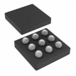 CSD75204W15
The activity of extra discounts on wholesale prices is in full swing…
Please fill in your contact information and we will send you the latest wholesale price list.





