 ChipApex | Global Electronic Components Supplier
SEARCH
Search Product
Search Post
— IC芯片 | 连接器 | 传感器 | 被动器件 —
Search productSearch post
— IC芯片 | 连接器 | 传感器 | 被动器件 —
Consult the customer manager about the wholesale price.
consultation hotline:86-132-6715-2157
email:[email protected]
Contact the product manager for consultation. One-stop consultation is available.
Do you want a lower wholesale price? Please send us your inquiry and we will reply immediately.
The CSD75211W1723 is a dual P-channel NexFET power MOSFET array in a 12-DSBGA package. It features a -20V drain-source voltage and a continuous drain current of -4.5A. The device offers an ultra-low on-resistance, with RDS(on) reaching 32mΩ at VGS = -4.5V and 40mΩ at VGS = -2.5V. Total gate charge (Qg) is 4.5nC at -4.5V, supporting high-speed switching. Power dissipation is rated at 1.5W, with a junction temperature range from -55°C to 150°C.
Verify the component status before procurement as the part may be discontinued. Confirm that the specific ordering suffix matches the required packaging format. Ensure compliance with RoHS and REACH standards during integration. Validate thermal resistance parameters against the actual PCB copper area used in the final application design.
Select this component for space-constrained battery-operated applications requiring low profile and minimal footprint. Evaluate the thermal resistance based on the minimum versus maximum copper mounting area requirements. Consider the logic-level gate drive thresholds when designing the control circuitry for optimal conduction characteristics.
This device belongs to the NexFET family, designed to deliver low on-resistance and gate charge within a small outline. It utilizes a wafer level package to minimize board space while maintaining necessary thermal characteristics for load management tasks.
CSD86311W1723
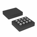 CSD75211W1723
The activity of extra discounts on wholesale prices is in full swing…
Please fill in your contact information and we will send you the latest wholesale price list.





