ChipApex | Global Electronic Components Supplier

SEARCH
Search Product
Search Post
— IC芯片 | 连接器 | 传感器 | 被动器件 —
Search productSearch post
— IC芯片 | 连接器 | 传感器 | 被动器件 —
Consult the customer manager about the wholesale price.
consultation hotline:86-132-6715-2157
email:[email protected]
Contact the product manager for consultation. One-stop consultation is available.
Do you want a lower wholesale price? Please send us your inquiry and we will reply immediately.
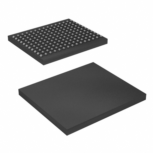
CY7C1565KV18-450BZXI is listed in the Memory IC range at ChipApex. The manufacturer field lists Infineon Technologies. Its product description is IC SRAM 72MBIT PAR 165FBGA. Review the specifications below when checking this part for your BOM.
The CY7C1565KV18 is a 72-Mbit QDR II+ synchronous SRAM organized as 2M x 36. It features a maximum operating frequency of 450 MHz and supports concurrent read and write transactions via separate independent ports. The device utilizes a four-word burst architecture with 2.5-cycle read latency when the DOFF pin is asserted HIGH. It operates on a 1.8 V core supply (± 0.1 V) and accepts I/O voltages between 1.4 V and 1.9 V. The component is housed in a 165-ball FBGA package measuring 13 × 15 mm.
Verify the specific speed grade suffix matches the required clock frequency, as the base part number covers multiple variants up to 550 MHz. Confirm the package marking code corresponds to the 165-ball FBGA configuration. Ensure the ordering suffix aligns with the desired temperature range and RoHS compliance status before finalizing procurement orders.
Select this component when system design requires simultaneous independent read and write access without data contention. The 2.5-cycle latency mode is optimal for high-throughput applications, while disabling the PLL allows compatibility with legacy QDR I timing constraints. Verify that the host controller supports the required DDR interface signaling and echo clock synchronization.
This device belongs to the Cypress/Infineon QDR II+ SRAM family, which extends the original QDR architecture by adding programmable impedance and enhanced timing features. It shares the same physical footprint and basic pinout structure as other members in the 72-Mbit density class, facilitating direct board-level upgrades within compatible memory subsystems.
Direct substitutes include CY7C1565KV18-400BZXI and CY7C1565KV18-550BZXI, which share identical pinouts and functionality but differ in maximum clock frequency specifications.
Asserting DOFF HIGH enables the standard 2.5-cycle read latency. Connecting DOFF LOW disables the internal PLL, causing the device to operate in QDR I mode with one-cycle read latency.
The ZQ pin is used for output impedance matching. An external resistor connected between ZQ and ground tunes the output drivers to match the system data bus impedance.
Explore related parts through Memory, Integrated Circuits (ICs), all product categories, ChipApex homepage.
 CY7C1565KV18-450BZXI
CY7C1565KV18-450BZXI is listed in the Memory IC range at ChipApex. The manufacturer field lists Infineon Technologies. Its product description is IC SRAM 72MBIT PAR…
Read More
CY7C1565KV18-450BZXI is listed in the Memory IC range at ChipApex. The manufacturer field lists Infineon Technologies. Its product description is IC SRAM 72MBIT PAR…
Read More
CY7C1565KV18-450BZXI is listed in the Memory IC range at ChipApex. The manufacturer field lists Infineon Technologies. Its product description is IC SRAM 72MBIT PAR…
Read More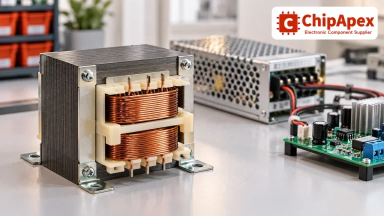
Select power transformers by input frequency, secondary VA, rectifier load, isolation, regulation and inrush. Build a clearer specification for your next RFQ.
Read More
CY7C1565KV18-450BZXI is listed in the Memory IC range at ChipApex. The manufacturer field lists Infineon Technologies. Its product description is IC SRAM 72MBIT PAR…
Read More
CY7C1565KV18-450BZXI is listed in the Memory IC range at ChipApex. The manufacturer field lists Infineon Technologies. Its product description is IC SRAM 72MBIT PAR…
Read More
Compare RC, crystal and MEMS oscillator circuits. Check ppm, jitter, load capacitance, startup margin and output compatibility before choosing a clock source.
Read More
CY7C1565KV18-450BZXI is listed in the Memory IC range at ChipApex. The manufacturer field lists Infineon Technologies. Its product description is IC SRAM 72MBIT PAR…
Read More
CY7C1565KV18-450BZXI is listed in the Memory IC range at ChipApex. The manufacturer field lists Infineon Technologies. Its product description is IC SRAM 72MBIT PAR…
Read More
CY7C1565KV18-450BZXI is listed in the Memory IC range at ChipApex. The manufacturer field lists Infineon Technologies. Its product description is IC SRAM 72MBIT PAR…
Read More
CY7C1565KV18-450BZXI is listed in the Memory IC range at ChipApex. The manufacturer field lists Infineon Technologies. Its product description is IC SRAM 72MBIT PAR…
Read More
CY7C1565KV18-450BZXI is listed in the Memory IC range at ChipApex. The manufacturer field lists Infineon Technologies. Its product description is IC SRAM 72MBIT PAR…
Read More
The activity of extra discounts on wholesale prices is in full swing…
Please fill in your contact information and we will send you the latest wholesale price list.