 ChipApex | Global Electronic Components Supplier
SEARCH
Search Product
Search Post
— IC芯片 | 连接器 | 传感器 | 被动器件 —
Search productSearch post
— IC芯片 | 连接器 | 传感器 | 被动器件 —
Consult the customer manager about the wholesale price.
consultation hotline:86-132-6715-2157
email:[email protected]
Contact the product manager for consultation. One-stop consultation is available.
Do you want a lower wholesale price? Please send us your inquiry and we will reply immediately.
The DMC2025UFDBQ-13 is a complementary pair enhancement mode MOSFET manufactured by Diodes Incorporated. It integrates an N-channel and a P-channel device within a single U-DFN2020-6 package. The N-channel component provides a drain-source breakdown voltage of 20V, with a maximum continuous drain current of 6.0A at +25°C and a static on-resistance of 25mΩ at VGS = 4.5V. The P-channel component offers a -20V breakdown voltage, supporting a maximum continuous drain current of -3.5A at +25°C and a static on-resistance of 75mΩ at VGS = -4.5V. The device operates across a temperature range of -55°C to +150°C.
Verify the specific ordering suffix '-13' corresponds to the required tape and reel quantity of 10,000 units before finalizing procurement plans. Confirm that the U-DFN2020-6 (Type B) package dimensions align with the target printed circuit board layout. Ensure compliance with RoHS 3 directives and verify that the NiPdAu terminal finish meets the solderability requirements of MIL-STD-208 Method 208.
Select this component when designing circuits requiring a matched N-channel and P-channel MOSFET pair in a minimal footprint. The low on-resistance characteristics support efficient power switching in portable applications. Verify that the gate threshold voltages are compatible with the intended logic levels. Consider the thermal resistance values when calculating heat dissipation under steady-state operating conditions.
This part belongs to the DMC2025UFDBQ family of complementary enhancement mode MOSFETs. The '-13' suffix specifically denotes the packaging format containing 10,000 units per tape and reel, whereas the '-7' suffix indicates a 3,000-unit reel. Both variants share identical electrical specifications and physical dimensions.
Direct replacements must match the U-DFN2020-6 package and provide equivalent N-channel and P-channel performance metrics. Verify that any substitute component maintains AEC-Q101 qualification if automotive reliability is required. Check for compatibility with existing PCB footprints and ensure similar thermal resistance ratings.
The maximum continuous drain current for the N-channel component is 6.0A at an ambient temperature of +25°C.
Yes, the operating and storage temperature range extends from -55°C to +150°C.
The N-channel on-resistance increases from 25mΩ at VGS = 4.5V to 35mΩ at VGS = 2.5V. The P-channel on-resistance increases from 75mΩ at VGS = -4.5V to 140mΩ at VGS = -2.5V.
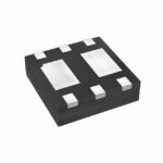 DMC2025UFDBQ-13
The activity of extra discounts on wholesale prices is in full swing…
Please fill in your contact information and we will send you the latest wholesale price list.





