ChipApex | Global Electronic Components Supplier
SEARCH
Search Product
Search Post
— IC芯片 | 连接器 | 传感器 | 被动器件 —
Search productSearch post
— IC芯片 | 连接器 | 传感器 | 被动器件 —
Consult the customer manager about the wholesale price.
consultation hotline:86-132-6715-2157
email:[email protected]
Contact the product manager for consultation. One-stop consultation is available.
Do you want a lower wholesale price? Please send us your inquiry and we will reply immediately.
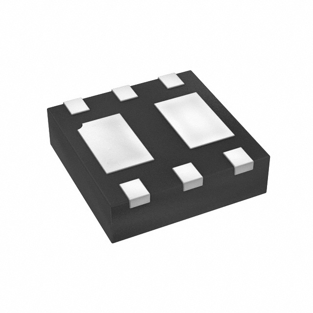
The DMC2053UFDB is a complementary pair enhancement mode MOSFET manufactured by Diodes Incorporated. It integrates an N-channel and a P-channel device within a single U-DFN2020-6 package. The N-channel component provides a maximum drain-source voltage of 20V, with an on-resistance of 35mΩ at VGS=4.5V and a continuous drain current of 4.6A. The P-channel counterpart offers a -20V breakdown voltage, featuring an on-resistance of 75mΩ at VGS=-4.5V and a continuous drain current of -3.1A. Designed for high-efficiency power management, the device maintains low input capacitance and superior switching performance.
Verify the specific ordering suffix to confirm packaging quantity. The -7 suffix indicates a tape and reel carrier containing 3,000 units per reel. Confirm compliance requirements such as RoHS and halogen-free status directly from the manufacturer's documentation before finalizing procurement specifications.
Select this component when space-constrained designs require integrated N-channel and P-channel logic-level MOSFETs. Ensure the application gate drive voltage aligns with the specified thresholds for optimal RDS(ON) performance. Verify that the thermal dissipation requirements are met using the provided junction-to-ambient thermal resistance values under the intended PCB copper layout conditions.
This part belongs to the DMC2053 series of complementary enhancement mode MOSFETs. It is designed specifically for applications requiring small form factors and high efficiency. The standard commercial version is distinguished from automotive-compliant variants, which are documented under separate datasheets and carry different ordering suffixes.
An automotive-compliant alternative exists under the part number DMC2053UFDBQ. Verify if the specific reliability standards required for the target application necessitate the automotive-grade variant over the standard commercial DMC2053UFDB.
The device supports an operating and storage temperature range from -55°C to +150°C.
The P-channel on-resistance is 75mΩ at VGS = -4.5V, increases to 110mΩ at VGS = -2.5V, and reaches 168mΩ at VGS = -1.8V.
The total gate charge (Qg) for the N-channel device is 7.7nC when tested at VDS = 10V, ID = 6A, and VGS = 10V.
 DMC2053UFDB-7
The activity of extra discounts on wholesale prices is in full swing…
Please fill in your contact information and we will send you the latest wholesale price list.