 ChipApex | Global Electronic Components Supplier
SEARCH
Search Product
Search Post
— IC芯片 | 连接器 | 传感器 | 被动器件 —
Search productSearch post
— IC芯片 | 连接器 | 传感器 | 被动器件 —
Consult the customer manager about the wholesale price.
consultation hotline:86-132-6715-2157
email:[email protected]
Contact the product manager for consultation. One-stop consultation is available.
Do you want a lower wholesale price? Please send us your inquiry and we will reply immediately.
The DMC2450UV-13 is a complementary pair enhancement mode MOSFET from Diodes Incorporated, housed in an SOT563 surface-mount package. It integrates an N-channel device (Q1) and a P-channel device (Q2). Q1 features a drain-source voltage of 20V, with a maximum on-resistance of 0.5Ω at VGS=4.5V and 0.9Ω at VGS=1.8V. Q2 has a -20V rating, with maximum on-resistance of 1.0Ω at VGS=-4.5V and 2.0Ω at VGS=-1.8V. The component operates within a temperature range of -55°C to +150°C.
Verify the specific ordering suffix against official documentation to confirm packaging quantity and reel specifications. Confirm RoHS compliance status and lead-free characteristics directly with the manufacturer or authorized distributors before procurement. Ensure the selected variant matches the required tape and reel format for automated assembly processes.
Select this component for designs requiring a compact complementary MOSFET pair in an SOT563 footprint. Evaluate thermal resistance values based on the specific PCB copper area and mounting conditions. Consider the gate threshold voltage limits when designing control circuits for low-voltage battery systems.
This part belongs to Diodes Incorporated's generation of complementary MOSFETs designed to minimize on-state resistance while maintaining superior switching performance. The DMC2450UV series specifically targets high-efficiency power management applications where space constraints and low power consumption are critical design parameters.
DMC2450UV-7
The maximum continuous drain current for the N-channel device (Q1) is 1,030 mA at TA = +25°C with VGS = 4.5V.
Yes, the datasheet specifies that both the N-channel and P-channel devices feature ESD protected gates.
The typical input capacitance (Ciss) for the N-channel device is 37.1 pF, measured at VDS = 10V and f = 1.0MHz.
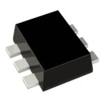 DMC2450UV-13
The activity of extra discounts on wholesale prices is in full swing…
Please fill in your contact information and we will send you the latest wholesale price list.





