 ChipApex | Global Electronic Components Supplier
SEARCH
Search Product
Search Post
— IC芯片 | 连接器 | 传感器 | 被动器件 —
Search productSearch post
— IC芯片 | 连接器 | 传感器 | 被动器件 —
Consult the customer manager about the wholesale price.
consultation hotline:86-132-6715-2157
email:[email protected]
Contact the product manager for consultation. One-stop consultation is available.
Do you want a lower wholesale price? Please send us your inquiry and we will reply immediately.
The DMC2710UV-7 is a complementary pair enhancement mode MOSFET manufactured by Diodes Incorporated. It integrates one N-channel and one P-channel device in an SOT563 surface-mount package. The N-channel transistor (Q1) supports a drain-source voltage of 20V with a maximum continuous drain current of 1.1A at +25°C, while the P-channel transistor (Q2) provides -20V breakdown and -0.8A current capability. Key electrical parameters include a typical on-resistance of 0.4Ω for Q1 and 0.7Ω for Q2 at VGS = ±4.5V. The component operates within a junction temperature range of -55°C to +150°C.
Verify the specific ordering suffix against official documentation to confirm packaging details. The standard tape and reel configuration typically contains 3000 units per reel. Confirm that the component meets RoHS compliance requirements and ensure proper handling procedures are followed due to ESD sensitivity. Cross-reference the manufacturer's datasheet revision history for any updates to mechanical or electrical specifications before finalizing procurement orders.
Select this component when space-constrained designs require a matched N/P-channel pair in a single SOT563 footprint. Ensure the application logic levels align with the low gate threshold voltages specified. Evaluate thermal dissipation capabilities based on the junction-to-ambient resistance values provided in the datasheet. Verify that the required switching speeds and capacitance characteristics meet the system's dynamic performance requirements.
This part belongs to Diodes Incorporated's portfolio of small-signal MOSFETs designed for portable electronics and power management applications. The SOT563 package allows for high-density PCB layouts compared to larger discrete packages. It serves as a compact solution for load switching and level shifting tasks where dual polarity control is necessary within a minimal physical envelope.
Direct replacements must match the SOT563 pinout and complementary N/P-channel configuration. Verify that substitute components offer equivalent or superior BVDSS ratings and comparable RDS(ON) values at the intended operating gate voltages. Thermal resistance and package dimensions should be checked to ensure compatibility with existing board footprints.
The maximum continuous drain current for the N-channel device (Q1) is 1.1A at an ambient temperature of +25°C.
Yes, the datasheet specifies that the gates are ESD protected.
The typical input capacitance (Ciss) for the N-channel transistor is 42 pF, measured at VDS = 16V and f = 1.0MHz.
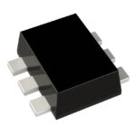 DMC2710UV-7
The activity of extra discounts on wholesale prices is in full swing…
Please fill in your contact information and we will send you the latest wholesale price list.





