 ChipApex | Global Electronic Components Supplier
SEARCH
Search Product
Search Post
— IC芯片 | 连接器 | 传感器 | 被动器件 —
Search productSearch post
— IC芯片 | 连接器 | 传感器 | 被动器件 —
Consult the customer manager about the wholesale price.
consultation hotline:86-132-6715-2157
email:[email protected]
Contact the product manager for consultation. One-stop consultation is available.
Do you want a lower wholesale price? Please send us your inquiry and we will reply immediately.
The DMC3016LSD-13 is a complementary pair enhancement mode MOSFET in an SO-8 package. It integrates one N-channel and one P-channel device. The N-channel Q1 has a drain-source voltage of 30V, on-resistance of 16mΩ at VGS=10V, and continuous current of 8.2A. The P-channel Q2 has a breakdown voltage of -30V, on-resistance of 28mΩ at VGS=-10V, and continuous current of -6.2A. Total power dissipation is 1.2W at +25°C. Operating temperature ranges from -55°C to +150°C.
Verify the datasheet revision (DS36935 Rev. 4) matches the production batch. Confirm the suffix '-13' indicates tape and reel packaging with 2,500 units per reel. Ensure compliance with RoHS 2 and J-STD-020 moisture sensitivity level 1 requirements during storage and soldering processes.
Select this component when a matched N/P pair is required for synchronous rectification or load switching. Verify that the 30V rating accommodates system transients. Check thermal resistance values against the PCB copper area available for heat dissipation to ensure junction temperatures remain within limits.
This part belongs to the DMC3016 series of complementary MOSFETs manufactured by Diodes Incorporated. It utilizes a standard SO-8 surface mount case with a molded plastic green molding compound. The product marking includes the code C3016LD followed by date codes.
DMC3016LDV-13
The gate threshold voltage ranges from 1.0V to 3.0V for both the N-channel and P-channel devices.
For the N-channel, RDS(ON) is 16mΩ at VGS=10V and 20mΩ at VGS=4.5V. For the P-channel, it is 28mΩ at VGS=-10V and 38mΩ at VGS=-4.5V.
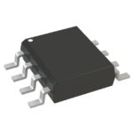 DMC3016LSD-13
The activity of extra discounts on wholesale prices is in full swing…
Please fill in your contact information and we will send you the latest wholesale price list.





