 ChipApex | Global Electronic Components Supplier
SEARCH
Search Product
Search Post
— IC芯片 | 连接器 | 传感器 | 被动器件 —
Search productSearch post
— IC芯片 | 连接器 | 传感器 | 被动器件 —
Consult the customer manager about the wholesale price.
consultation hotline:86-132-6715-2157
email:[email protected]
Contact the product manager for consultation. One-stop consultation is available.
Do you want a lower wholesale price? Please send us your inquiry and we will reply immediately.
The DMG1029SV-7 is a complementary pair enhancement mode MOSFET in an SOT563 package. It integrates an N-channel device (Q1) and a P-channel device (Q2). Q1 offers a maximum drain-source voltage of 60V, with on-resistance values of 1.7Ω at VGS=10V and 3Ω at VGS=4.5V. Q2 provides -60V breakdown, with on-resistance values of 4Ω at VGS=-10V and 6Ω at VGS=-4.5V. The component operates within a temperature range of -55°C to +150°C.
Verify the specific ordering suffix when purchasing. The standard version uses the '-7' suffix, while the automotive qualified version utilizes the 'Q-7' suffix. Confirm that the required part matches the intended application grade before procurement.
Select this component for low-voltage switching tasks requiring minimal footprint. Ensure gate drive voltages align with the specified thresholds for optimal on-resistance. Verify thermal dissipation requirements against the junction-to-ambient resistance limits provided in the datasheet.
This device belongs to the DMG1029 series of complementary MOSFETs manufactured by Diodes Incorporated. It is designed to minimize on-state resistance while maintaining superior switching performance, making it suitable for high-efficiency power management applications.
The DMG1029SVQ-7 serves as the automotive-grade equivalent. Both parts share identical electrical and thermal characteristics, differing only in qualification standards.
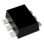 DMG1029SV-7
The activity of extra discounts on wholesale prices is in full swing…
Please fill in your contact information and we will send you the latest wholesale price list.





