 ChipApex | Global Electronic Components Supplier
SEARCH
Search Product
Search Post
— IC芯片 | 连接器 | 传感器 | 被动器件 —
Search productSearch post
— IC芯片 | 连接器 | 传感器 | 被动器件 —
Consult the customer manager about the wholesale price.
consultation hotline:86-132-6715-2157
email:[email protected]
Contact the product manager for consultation. One-stop consultation is available.
Do you want a lower wholesale price? Please send us your inquiry and we will reply immediately.
The DMG6301UDW-7 is a dual N-channel enhancement mode MOSFET manufactured by Diodes Incorporated. It features a maximum drain-source voltage (V(BR)DSS) of 25 V and a gate-source voltage (VGSS) rating of 8 V. The device provides a continuous drain current (ID) of 0.24 A at VGS = 4.5 V and 0.22 A at VGS = 2.7 V, with a typical static drain-source on-resistance (RDS(ON)) of 4 Ω at VGS = 4.5 V and 5 Ω at VGS = 2.7 V. Total power dissipation is rated at 0.3 W to 0.37 W depending on the PCB layout. The component operates within a junction temperature range of -55°C to +150°C and utilizes an SOT-363 surface-mount package.
Verify the specific ordering suffix against official documentation before procurement. The standard suffix indicates a 3,000-unit tape and reel packaging format. Confirm that the requested revision matches the required design specifications. Ensure compliance with RoHS and halogen-free requirements if mandated by the project. Cross-reference the manufacturer part number with authorized distributor listings to validate authenticity.
Select this component when a dual N-channel topology is required in a minimal footprint. Evaluate the 4 Ω RDS(ON) specification against the target load current to ensure thermal limits are not exceeded. Consider the 25 V breakdown voltage relative to the system supply rails. Verify that the SOT-363 package dimensions fit the available board space constraints.
This component belongs to the DMG series of dual MOSFETs from Diodes Incorporated. It serves as a complementary solution for low-voltage switching applications where space is limited. The device integrates two independent N-channel FETs, allowing for differential or bridge configurations without requiring separate discrete components.
Check for pin-compatible alternatives within the same SOT-363 form factor. Verify that substitute parts meet or exceed the 25 V drain-source voltage and 0.24 A continuous current ratings. Ensure the replacement maintains similar gate threshold voltage characteristics for compatible logic drive levels.
The maximum gate-source voltage (VGSS) rating is 8 V.
Yes, the DMG6301UDW includes integrated gate protection diodes capable of withstanding greater than 6kV via the Human Body Model.
The total gate charge (Qg) is typically 0.36 nC under test conditions of VGS = 4.5 V, VDS = 5 V, and ID = 0.2 A.
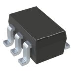 DMG6301UDW-7
The activity of extra discounts on wholesale prices is in full swing…
Please fill in your contact information and we will send you the latest wholesale price list.





