 ChipApex | Global Electronic Components Supplier
SEARCH
Search Product
Search Post
— IC芯片 | 连接器 | 传感器 | 被动器件 —
Search productSearch post
— IC芯片 | 连接器 | 传感器 | 被动器件 —
Consult the customer manager about the wholesale price.
consultation hotline:86-132-6715-2157
email:[email protected]
Contact the product manager for consultation. One-stop consultation is available.
Do you want a lower wholesale price? Please send us your inquiry and we will reply immediately.
The DMG6302UDW-13 is a dual P-channel enhancement mode MOSFET manufactured by Diodes Incorporated in an SOT-363 package. It features a drain-source voltage (BVDSS) of -25V and a continuous drain current (ID) of -150mA at VGS = -4.5V. The maximum on-resistance (RDS(ON)) is 10Ω at VGS = -4.5V and 13Ω at VGS = -2.7V. Gate-source voltage (VGSS) is rated at ±8V, with a gate threshold voltage (VGS(TH)) ranging from -0.65V to -1.5V. Total gate charge (Qg) is typically 0.34nC. Power dissipation is 310mW on FR-4 PCB with minimum pads, or 380mW on high copper coverage boards. Operating temperature ranges from -55°C to +150°C.
Verify the ordering suffix '-13' corresponds to the 10,000-unit tape and reel packaging format specified in the datasheet. Confirm that the component meets environmental requirements such as being lead-free, halogen-free, and antimony-free. Ensure the application design accounts for the thermal resistance values provided for different PCB copper coverage scenarios.
Select this component when a dual P-channel MOSFET is required in a small footprint. Evaluate the RDS(ON) specifications against the load current requirements at the intended gate drive voltage (-2.7V or -4.5V). Consider the power dissipation limits and thermal resistance characteristics relative to the PCB layout and ambient operating conditions.
This part belongs to the DMG series of dual P-channel enhancement mode MOSFETs from Diodes Incorporated. It shares the SOT-363 case style with other devices in the family but is distinguished by its specific voltage and current ratings. The '-13' suffix indicates a specific tape and reel quantity for manufacturing integration.
The datasheet lists the DMG6302UDW-7 as an equivalent part number within the same product line, differing only in the tape and reel packaging quantity (3,000 units versus 10,000 units). Verify pinout compatibility and electrical parameters before substituting with other dual P-channel MOSFETs from different manufacturers.
The maximum continuous drain current is -150mA when VGS is -4.5V and the device is mounted on a 1” x 1” FR-4 PCB with high coverage 2oz copper.
The maximum RDS(ON) is 10Ω at VGS = -4.5V and increases to 13Ω at VGS = -2.7V, both measured at ID = -0.14A and -0.05A respectively.
Standard production is not explicitly qualified for automotive use. For automotive applications requiring AEC-Q100/101/200 qualification and IATF 16949 manufacturing, customers must contact Diodes Incorporated directly.
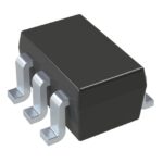 DMG6302UDW-13
The activity of extra discounts on wholesale prices is in full swing…
Please fill in your contact information and we will send you the latest wholesale price list.





