 ChipApex | Global Electronic Components Supplier
SEARCH
Search Product
Search Post
— IC芯片 | 连接器 | 传感器 | 被动器件 —
Search productSearch post
— IC芯片 | 连接器 | 传感器 | 被动器件 —
Consult the customer manager about the wholesale price.
consultation hotline:86-132-6715-2157
email:[email protected]
Contact the product manager for consultation. One-stop consultation is available.
Do you want a lower wholesale price? Please send us your inquiry and we will reply immediately.
The DMG6302UDW-7 is a dual P-channel enhancement mode MOSFET manufactured by Diodes Incorporated in an SOT-363 surface-mount package. It features a drain-source voltage (BVDSS) of -25V and a continuous drain current (ID) of -150mA at +25°C with VGS = -4.5V. The maximum on-resistance (RDS(ON)) is 10Ω at VGS = -4.5V and 13Ω at VGS = -2.7V. Key electrical parameters include a gate threshold voltage (VGS(TH)) ranging from -0.65V to -1.5V, total gate charge (Qg) of 0.34nC, and input capacitance (Ciss) of 30.7pF. Power dissipation is rated at 310mW on minimal pads and 380mW on high-copper boards, with an operating temperature range of -55°C to +150°C.
Verify component authenticity through authorized Diodes Incorporated distributors or certified supply chain partners. Confirm datasheet revision DS37498 Rev. 3-2 matches physical markings. Ensure packaging specifications align with tape and reel requirements for automated assembly processes. Validate compliance with RoHS directives and halogen-free standards prior to integration into final products.
Select this component when dual P-channel isolation is required in compact SOT-363 footprints. Evaluate RDS(ON) performance against specific gate drive voltages (-2.7V vs -4.5V) to ensure adequate current handling. Consider thermal resistance values based on PCB copper coverage and ambient operating conditions. Verify that the -25V breakdown voltage exceeds peak circuit transients.
This part belongs to the DMG6302UDW series of dual P-channel MOSFETs from Diodes Incorporated. It shares the SOT-363 mechanical outline with other dual-channel variants but differs in channel type and specific electrical ratings. The product line targets space-constrained designs requiring multiple switching elements on a single substrate.
Direct substitutes require matching dual P-channel topology, SOT-363 footprint, and compatible -25V BVDSS ratings. Verify pinout compatibility and thermal characteristics before substitution. Cross-reference specific RDS(ON) limits at intended gate drive voltages to maintain circuit performance.
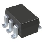 DMG6302UDW-7
The activity of extra discounts on wholesale prices is in full swing…
Please fill in your contact information and we will send you the latest wholesale price list.





