 ChipApex | Global Electronic Components Supplier
SEARCH
Search Product
Search Post
— IC芯片 | 连接器 | 传感器 | 被动器件 —
Search productSearch post
— IC芯片 | 连接器 | 传感器 | 被动器件 —
Consult the customer manager about the wholesale price.
consultation hotline:86-132-6715-2157
email:[email protected]
Contact the product manager for consultation. One-stop consultation is available.
Do you want a lower wholesale price? Please send us your inquiry and we will reply immediately.
The DMHC6070LSD-13 is a complementary enhancement mode MOSFET H-Bridge from Diodes Incorporated, packaged in an SOIC-8 case. It integrates two N-channel and two P-channel devices. The N-channel features a drain-source breakdown voltage of 60V, with on-resistance values of 100mΩ at VGS=10V and 120mΩ at VGS=4.5V. Continuous drain current reaches 4.1A at 25°C for the N-channel and 3.1A for the P-channel. The P-channel exhibits on-resistances of 170mΩ at VGS=-10V and 250mΩ at VGS=-4.5V. Total power dissipation is rated at 1.6W, with an operating temperature range spanning -55°C to +150°C.
Verify the component against the official Diodes Incorporated datasheet DS38714 Rev. 1-2 to confirm electrical parameters and pinout compatibility. Ensure that the SO-8 packaging and tape & reel specifications align with automated assembly requirements. Cross-reference maximum ratings such as thermal resistance and avalanche energy to validate suitability for the target circuit environment.
Select this device for designs requiring a compact complementary MOSFET solution. Evaluate the specific on-resistance requirements at the intended gate drive voltage, noting the difference between 10V and 4.5V operation. Consider the total power dissipation limits and thermal resistance characteristics when determining heat sinking needs for continuous duty cycles.
This part belongs to the DMHC6070 series of complementary enhancement mode MOSFETs manufactured by Diodes Incorporated. It is designed specifically for H-Bridge configurations, combining both N-channel and P-channel technologies into one package to reduce board space and simplify driver design compared to discrete solutions.
Consult the manufacturer's documentation for officially confirmed substitute part numbers. Verify that any alternative maintains identical pin configuration, voltage ratings, and thermal performance before implementation.
The N-channel has a typical RDS(ON) of 60mΩ at VGS=10V and 70mΩ at VGS=4.5V, with maximum values of 100mΩ and 120mΩ respectively.
The P-channel RDS(ON) is typically 120mΩ at VGS=-10V and increases to 170mΩ at VGS=-4.5V.
The N-channel supports up to 4.1A at TA=+25°C, while the P-channel supports up to 3.1A under the same conditions.
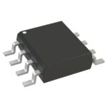 DMHC6070LSD-13
The activity of extra discounts on wholesale prices is in full swing…
Please fill in your contact information and we will send you the latest wholesale price list.





