 ChipApex | Global Electronic Components Supplier

SEARCH
Search Product
Search Post
— IC芯片 | 连接器 | 传感器 | 被动器件 —
Search productSearch post
— IC芯片 | 连接器 | 传感器 | 被动器件 —
Consult the customer manager about the wholesale price.
consultation hotline:86-132-6715-2157
email:[email protected]
Contact the product manager for consultation. One-stop consultation is available.
Do you want a lower wholesale price? Please send us your inquiry and we will reply immediately.
The DMN2023UCB4-7 is a dual N-channel enhancement mode field MOSFET manufactured by Diodes Incorporated. It features a source-to-source configuration within an X1-WLB1818-4 package. Key electrical parameters include a maximum source-to-source voltage of 24V and a continuous source current of 6.0A at +25°C. The static source-to-source on-resistance (RSS(ON)) is typically 26mΩ at VGS = 4.5V and IS = 3.0A, with a maximum of 29mΩ at VGS = 3.7V. Gate threshold voltage ranges from 0.5V to 1.3V. Total gate charge is typically 29nC at VGS = 4.5V and VSS = 10V. The device operates within a junction temperature range of -55°C to +150°C.
Verify the specific ordering suffix '-7' corresponds to the 3,000-unit tape and reel packaging format. Confirm that the component meets RoHS compliance and is halogen-free if required by the manufacturing process. Ensure the design accommodates the X1-WLB1818-4 package dimensions and moisture sensitivity level 1 requirements during storage and assembly.
Select this component when a compact dual N-channel solution is required for low-voltage applications. The 24V rating and 6A continuous current capability suit portable electronics. Evaluate the thermal resistance of 88.21°C/W against the expected power dissipation of 1.45W at +25°C. Consider the low gate charge for high-frequency switching needs.
This part belongs to Diodes Incorporated's generation of thin WLCSP MOSFETs designed for high-efficiency power management. It utilizes a specialized packaging process to reduce on-resistance while maintaining small footprint. The dual configuration allows for independent control or parallel operation within a minimal area, targeting space-constrained consumer devices.
Publicly confirmed substitute part numbers are not available in the provided documentation. Verify pinout compatibility and electrical parameter margins before considering alternative manufacturers or different package types.
The maximum source-to-source breakdown voltage (V(BR)SSS) is 24V.
The device includes a built-in G-S protection diode that provides ESD protection rated at 2kV under the Human Body Model (HBM) standard.
The typical total gate charge (Qg) is 29nC, measured at VGS = 4.5V and VSS = 10V with IS = 6A.
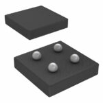 DMN2023UCB4-7

The activity of extra discounts on wholesale prices is in full swing…
Please fill in your contact information and we will send you the latest wholesale price list.





