ChipApex | Global Electronic Components Supplier

SEARCH
Search Product
Search Post
— IC芯片 | 连接器 | 传感器 | 被动器件 —
Search productSearch post
— IC芯片 | 连接器 | 传感器 | 被动器件 —
Consult the customer manager about the wholesale price.
consultation hotline:86-132-6715-2157
email:[email protected]
Contact the product manager for consultation. One-stop consultation is available.
Do you want a lower wholesale price? Please send us your inquiry and we will reply immediately.
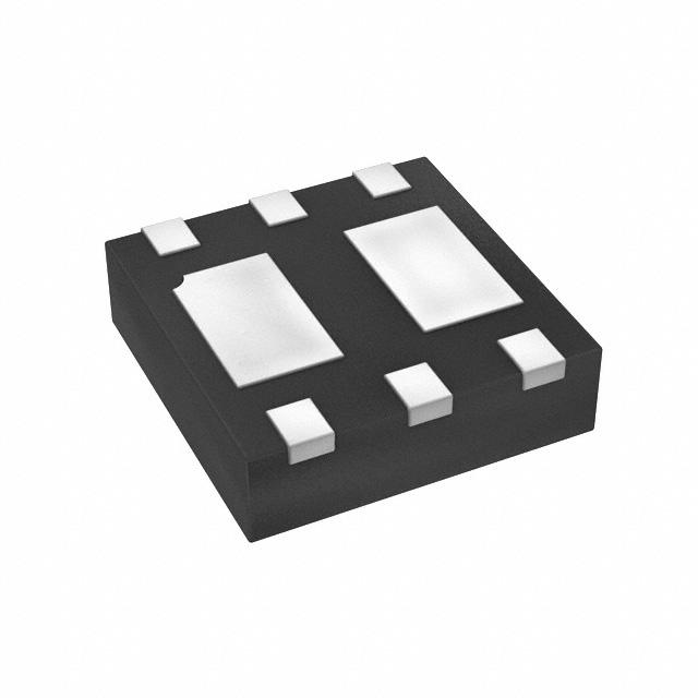
The DMN2041UFDB-13 is a dual N-channel enhancement mode MOSFET from Diodes Incorporated, housed in a U-DFN2020-6 (Type B) surface-mount package. It features a maximum drain-source voltage of 20V and a gate-source voltage rating of ±12V. At TA = +25°C, the continuous drain current reaches 4.7A at VGS = 4.5V and 3.7A at VGS = 2.5V. The static drain-source on-resistance is specified as 40mΩ max at VGS = 4.5V and 65mΩ max at VGS = 2.5V. Total gate charge is 8nC at VGS = 4.5V and 15nC at VGS = 8V. Operating and storage temperatures range from -55°C to +150°C.
Verify the specific ordering suffix against official documentation before purchase. The suffix indicates packaging quantity; for example, -13 denotes a 10,000-unit tape and reel, while -7 indicates a 3,000-unit reel. Confirm that the component meets all required environmental standards and automotive qualification criteria if applicable to the target application.
Select this component for applications requiring low on-state resistance and superior switching performance within a 20V system. Ensure the gate drive voltage aligns with the specified thresholds for optimal RDS(ON). Verify thermal management requirements based on the junction-to-ambient thermal resistance and expected power dissipation levels under steady-state or pulsed conditions.
This part belongs to the DMN2041 series of dual N-channel MOSFETs manufactured by Diodes Incorporated. It utilizes the U-DFN2020-6 (Type B) case style, designed for high-efficiency power management. The device integrates two independent N-channel transistors with built-in gate protection diodes in a single compact footprint.
Consult the manufacturer's official documentation for confirmed substitute part numbers. Cross-referencing requires matching electrical parameters such as BVDSS, RDS(ON), ID, and package dimensions to ensure functional compatibility without modification.
At TA = +70°C, the maximum continuous drain current decreases to 3.8A when VGS = 4.5V.
Yes, the DMN2041UFDB includes ESD protected gates with integrated gate protection diodes for both channels.
The typical body diode reverse recovery time is 6.6ns when tested at IS = 4.4A and dI/dt = 100A/μs.
 DMN2041UFDB-13

The activity of extra discounts on wholesale prices is in full swing…
Please fill in your contact information and we will send you the latest wholesale price list.