ChipApex | Global Electronic Components Supplier

SEARCH
Search Product
Search Post
— IC芯片 | 连接器 | 传感器 | 被动器件 —
Search productSearch post
— IC芯片 | 连接器 | 传感器 | 被动器件 —
Consult the customer manager about the wholesale price.
consultation hotline:86-132-6715-2157
email:[email protected]
Contact the product manager for consultation. One-stop consultation is available.
Do you want a lower wholesale price? Please send us your inquiry and we will reply immediately.
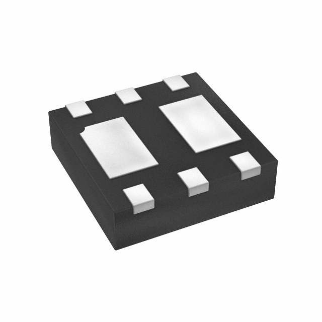
The DMN2050LFDB-7 is a dual N-channel enhancement mode MOSFET manufactured by Diodes Incorporated. It features a U-DFN2020-6 case with a maximum drain-source voltage (BVDSS) of 20V and a gate-source voltage (VGSS) of ±12V. The device provides a maximum continuous drain current (ID) of 4.5A at +25°C and 3.6A at +70°C. Static drain-source on-resistance (RDS(ON)) is rated at a maximum of 45mΩ at VGS = 4.5V and 55mΩ at VGS = 2.5V. Total power dissipation reaches 1.42W at +25°C, supported by a thermal resistance (RθJA) of 89°C/W.
Verify the specific ordering suffix when sourcing components. The -7 suffix indicates packaging in 3,000-unit tape and reels, whereas the -13 suffix denotes 10,000-unit reels. Confirm package type B specifications match design requirements before finalizing procurement orders.
Select this component for circuits requiring low on-resistance within a 20V limit. Ensure gate drive voltages align with the specified thresholds for optimal RDS(ON) performance. Evaluate thermal constraints carefully, as the U-DFN2020-6 package relies heavily on PCB copper area for effective heat dissipation during operation.
This part belongs to the DMN2050LFDB series of dual N-channel enhancement mode MOSFETs from Diodes Incorporated. It utilizes the U-DFN2020-6 Type B mechanical case, which offers a compact footprint suitable for space-constrained portable electronics and modern power management systems.
Publicly confirmed substitute part numbers are not available in the provided documentation. Verify pinout compatibility and electrical ratings against existing designs if considering alternative manufacturers or different package types.
The maximum continuous drain current is 4.5A at an ambient temperature of +25°C and decreases to 3.6A at +70°C.
The device supports an avalanche energy rating of 4.5 mJ with an inductance of 0.1mH and an avalanche current of 9A.
The typical turn-on delay time is 5 ns under test conditions of VDS = 10V, VGS = 4.5V, RG = 6Ω, and IDS = 1A.
 DMN2050LFDB-7

The activity of extra discounts on wholesale prices is in full swing…
Please fill in your contact information and we will send you the latest wholesale price list.