ChipApex | Global Electronic Components Supplier

SEARCH
Search Product
Search Post
— IC芯片 | 连接器 | 传感器 | 被动器件 —
Search productSearch post
— IC芯片 | 连接器 | 传感器 | 被动器件 —
Consult the customer manager about the wholesale price.
consultation hotline:86-132-6715-2157
email:[email protected]
Contact the product manager for consultation. One-stop consultation is available.
Do you want a lower wholesale price? Please send us your inquiry and we will reply immediately.
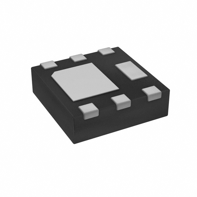
The DMN3025LFDF-7 is a surface-mount N-channel enhancement mode MOSFET manufactured by Diodes Incorporated. It features a drain-source voltage (Vdss) of 30 V and a maximum gate-source voltage (Vgs) of ±20 V. The device supports a continuous drain current (Id) of 8.3 A at steady state (+25°C) or 9.9 A for short durations (<10s). Its static drain-source on-resistance (Rds(on)) is specified as a maximum of 20.5 mΩ at Vgs = 10 V and Id = 7 A, and 30 mΩ at Vgs = 4.5 V. Total power dissipation reaches 2.1 W at +25°C with an exposed pad. The component operates within a junction temperature range of -55°C to +150°C.
Verify the specific ordering suffix against manufacturer documentation to confirm packaging quantity and reel specifications. Ensure that the procurement channel provides original manufacturer components to guarantee authenticity and adherence to quality standards. Confirm compliance requirements such as RoHS and REACH status match project specifications before finalizing orders.
Select this component when a compact N-channel MOSFET with low on-resistance is required for efficient power switching. Consider the 30V rating and 20.5mΩ Rds(on) for low-loss applications. Evaluate the U-DFN2020-6 package dimensions against PCB layout constraints. Verify thermal dissipation capabilities relative to the intended operating environment and heat sinking methods.
This part belongs to the DMN3025LFDF series of N-channel enhancement mode MOSFETs from Diodes Incorporated. It is designed for general-purpose interfacing and power management tasks. The device utilizes silicon technology and is housed in a U-DFN2020-6 (Type F) package. It is qualified to JEDEC standards for high reliability.
For automotive applications requiring specific change control, refer to the related automotive grade parts with the Q-suffix. Consult official substitution lists for electrically equivalent alternatives if this specific part number is unavailable.
The maximum gate-source voltage (VGSS) is rated at ±20 V.
Yes, the part is qualified to JEDEC standards for high reliability.
 DMN3025LFDF-7

The activity of extra discounts on wholesale prices is in full swing…
Please fill in your contact information and we will send you the latest wholesale price list.