 ChipApex | Global Electronic Components Supplier

SEARCH
Search Product
Search Post
— IC芯片 | 连接器 | 传感器 | 被动器件 —
Search productSearch post
— IC芯片 | 连接器 | 传感器 | 被动器件 —
Consult the customer manager about the wholesale price.
consultation hotline:86-132-6715-2157
email:[email protected]
Contact the product manager for consultation. One-stop consultation is available.
Do you want a lower wholesale price? Please send us your inquiry and we will reply immediately.
The DMN31D5UDW-13 is a dual N-channel enhancement mode MOSFET manufactured by Diodes Incorporated. It features a maximum drain-source voltage (BVDSS) of 30V and a gate-source voltage (VGSS) rating of ±12V. The device offers low on-state resistance, with RDS(ON) values ranging from 1.5Ω at VGS=4.5V to 4.5Ω at VGS=1.5V. Continuous drain current (ID) reaches 0.43A at VGS=4.5V under steady-state conditions at +25°C. Total power dissipation is rated at 0.33W or 0.43W depending on the PCB copper area. Operating temperature ranges from -55°C to +150°C.
Verify the specific ordering suffix '-13' corresponds to the 10,000-unit tape and reel packaging format. Confirm that the component meets all applicable environmental directives, including RoHS 3 and halogen-free requirements, before finalizing procurement specifications.
Select this component when space constraints require a dual N-channel MOSFET in an SOT363 footprint. Ensure the application logic levels align with the specified RDS(ON) thresholds, particularly if operating below 4.5V gate drive. Evaluate thermal performance against the junction-to-ambient resistance limits provided in the datasheet.
This part belongs to the DMN31 series of dual N-channel enhancement mode MOSFETs. It shares the same electrical characteristics as the DMN31D5UDW-7 variant, differing only in the standard manufacturing packing quantity. Both variants utilize the identical SOT363 package and silicon die design.
The DMN31D5UDW-7 serves as a direct functional substitute with identical electrical parameters and pinout. Verify that the alternative packaging quantity meets production needs without altering board layout or assembly processes.
The gate threshold voltage (VGS(TH)) typically ranges from 0.5V to 0.9V when tested at VDS = VGS and ID = 250μA.
RDS(ON) increases as gate voltage decreases. It is 1.5Ω max at 4.5V, 2.0Ω max at 2.5V, 3.0Ω max at 1.8V, and 4.5Ω max at 1.5V.
Yes, the forward voltage (VSD) is typically 0.7V and maximally 1.0V when sourced at 100mA with the gate shorted to the source.
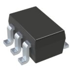 DMN31D5UDW-13

The activity of extra discounts on wholesale prices is in full swing…
Please fill in your contact information and we will send you the latest wholesale price list.





