 ChipApex | Global Electronic Components Supplier

SEARCH
Search Product
Search Post
— IC芯片 | 连接器 | 传感器 | 被动器件 —
Search productSearch post
— IC芯片 | 连接器 | 传感器 | 被动器件 —
Consult the customer manager about the wholesale price.
consultation hotline:86-132-6715-2157
email:[email protected]
Contact the product manager for consultation. One-stop consultation is available.
Do you want a lower wholesale price? Please send us your inquiry and we will reply immediately.
The DMN52D0UVT-7 is a dual N-channel enhancement mode MOSFET manufactured by Diodes Incorporated. It features a TSOT26 package with a drain-source voltage (BVDSS) of 50V and a maximum continuous drain current (ID) of 430mA at +25°C. The device offers low on-state resistance, specified as 2.0Ω max at VGS = 5.0V and 2.5Ω max at VGS = 2.5V. Key electrical parameters include a gate threshold voltage range of 0.49V to 1.0V, input capacitance of 41pF, and total gate charge of 0.7nC at VGS = 4.5V. Operating temperature ranges from -55°C to +150°C.
Verify the specific ordering suffix '-7' corresponds to the 3,000-unit reel packaging format when sourcing components. Confirm that the requested part matches the exact document number DS44923 Rev. 2 - 2 to ensure compatibility with design specifications. Check for any regional distribution restrictions or environmental compliance documentation required for your specific manufacturing location before finalizing procurement orders.
Select this component for applications requiring dual N-channel MOSFETs in ultra-small packages. Ensure the driving circuit can provide sufficient gate voltage to achieve the desired on-resistance levels, particularly at lower voltages like 1.8V or 2.5V. Consider the thermal resistance characteristics and power dissipation limits when designing the PCB layout to maintain safe operating temperatures under continuous load conditions.
This part belongs to the DMN52D0UVT series of dual N-channel enhancement mode MOSFETs. It shares similar electrical characteristics with other variants in the family but differs in packaging and tape-and-reel quantities. The TSOT26 package provides a space-saving solution compared to larger transistor packages while maintaining adequate thermal performance for low-power switching applications.
Direct substitutes may include other dual N-channel MOSFETs in TSOT26 packages with comparable BVDSS and ID ratings. Verify pinout compatibility and electrical parameter overlaps before implementation. Alternative packages such as SOT363 or X1-DFN1006-3 may require schematic redesign due to different pin configurations and thermal properties.
The maximum continuous drain current is 430mA at an ambient temperature of +25°C.
Yes, the internal schematic shows two independent N-channel MOSFETs, each with a built-in body diode between the source and drain terminals.
The typical input capacitance (Ciss) is 41pF, measured at VDS = 25V, VGS = 0V, and f = 1.0MHz.
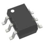 DMN52D0UVT-7

The activity of extra discounts on wholesale prices is in full swing…
Please fill in your contact information and we will send you the latest wholesale price list.





