 ChipApex | Global Electronic Components Supplier

SEARCH
Search Product
Search Post
— IC芯片 | 连接器 | 传感器 | 被动器件 —
Search productSearch post
— IC芯片 | 连接器 | 传感器 | 被动器件 —
Consult the customer manager about the wholesale price.
consultation hotline:86-132-6715-2157
email:[email protected]
Contact the product manager for consultation. One-stop consultation is available.
Do you want a lower wholesale price? Please send us your inquiry and we will reply immediately.
The DMN66D0LDW-7 is a dual N-channel enhancement mode MOSFET manufactured by Diodes Incorporated. It features a maximum drain-source voltage (BVDSS) of 60V and a continuous drain current (ID) of 115mA at +25°C. The device offers a typical on-resistance (RDS(on)) of 3.5Ω at VGS = 5V and 3.0Ω at VGS = 10V, with a maximum rating of 6Ω. It operates within a temperature range of -55°C to +150°C and has a total power dissipation of 250mW. Packaged in an SOT363 case, it includes ESD protection up to 1kV (HBM).
Verify the specific ordering suffix '-7' corresponds to the 3,000-unit tape and reel packaging format. Confirm that the component meets RoHS compliance and halogen-free requirements as specified in the datasheet notes. Ensure the application environment does not exceed the maximum junction temperature or power dissipation limits defined in the thermal characteristics section.
Select this component when a dual N-channel solution is required in a small surface mount package. Consider the 60V breakdown voltage and 115mA current capability against load requirements. Evaluate the RDS(on) performance at the intended gate drive voltage (5V or 10V) to ensure efficiency targets are met within the operating temperature range.
This part belongs to the DMN66 series of dual N-channel MOSFETs from Diodes Incorporated. It utilizes the SOT363 (Standard) case outline, which is also referred to as SC-88 in some distributor catalogs. The device is designed to minimize on-state resistance while maintaining superior switching performance compared to previous generations.
The automotive-compliant version is available under the separate part number DMN66D0LDWQ. Verify if AEC-Q qualification or PPAP capability is required for the target application before selecting the standard industrial grade part.
The continuous gate-source voltage (VGSS) is rated at ±20V.
The standard DMN66D0LDW-7 is qualified to JEDEC standards. For automotive applications requiring specific change control, the Q-suffix part (DMN66D0LDWQ) should be used.
The typical turn-off delay time (tD(off)) is 33ns under test conditions of VDD = 30V, ID = 0.115A, RL = 150Ω, and VGEN = 10V.
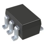 DMN66D0LDW-7

The activity of extra discounts on wholesale prices is in full swing…
Please fill in your contact information and we will send you the latest wholesale price list.





