ChipApex | Global Electronic Components Supplier

SEARCH
Search Product
Search Post
— IC芯片 | 连接器 | 传感器 | 被动器件 —
Search productSearch post
— IC芯片 | 连接器 | 传感器 | 被动器件 —
Consult the customer manager about the wholesale price.
consultation hotline:86-132-6715-2157
email:[email protected]
Contact the product manager for consultation. One-stop consultation is available.
Do you want a lower wholesale price? Please send us your inquiry and we will reply immediately.
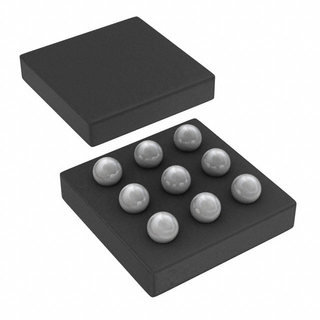
The DMP1011UCB9-7 is a P-channel enhancement mode MOSFET utilizing Diodes Incorporated's third-generation LD-MOS technology. It features an ultra-low on-state resistance of 8.2 mΩ and a total gate charge of 8.1 nC, enabling high-efficiency power transfer with minimal switching losses. The device operates with a drain-source voltage rating of -8 V and supports continuous drain currents up to -10 A at +25°C. Packaged in a compact U-WLB1515-9 chip-scale format measuring 1.5 mm × 1.5 mm with a height of 0.60 mm, it provides low thermal impedance for increased power density.
Verify the specific ordering suffix '-7' corresponds to the 3,000-unit tape and reel packaging configuration. Confirm that the component meets RoHS 2/3 compliance and is halogen-free. Ensure the application environment remains within the specified operating temperature range of -55°C to +150°C. Cross-reference the U-WLB1515-9 package dimensions with PCB layout guidelines to ensure proper soldering and thermal performance.
Select this component for applications requiring high current handling in extremely small footprints. The -8 V rating suits low-voltage systems where standard MOSFETs are too large. The low gate charge facilitates rapid switching in high-frequency converters. Consider the thermal resistance values when designing heat dissipation strategies for dense layouts.
This part belongs to Diodes Incorporated's DMP series of lateral MOSFETs. It utilizes the U-WLB1515-9 case style, which is a specialized chip-scale package designed for space-constrained designs. The product represents an advancement in LD-MOS technology aimed at reducing size while maintaining robust electrical performance.
Direct substitutes must match the -8 V rating, P-channel configuration, and U-WLB1515-9 package. Verify equivalent RDS(ON) and Qg values to maintain switching efficiency. Check if alternative packages require different PCB footprints.
The maximum pulsed drain current is -50 A, with a pulse duration of 10 μs and a duty cycle of ≤1%.
Yes, the DMP1011UCB9 is qualified to AEC-Q101 standards for high reliability.
The typical gate threshold voltage (VGS(th)) is -0.8 V at TA = +25°C.
 DMP1011UCB9-7

The activity of extra discounts on wholesale prices is in full swing…
Please fill in your contact information and we will send you the latest wholesale price list.