ChipApex | Global Electronic Components Supplier

SEARCH
Search Product
Search Post
— IC芯片 | 连接器 | 传感器 | 被动器件 —
Search productSearch post
— IC芯片 | 连接器 | 传感器 | 被动器件 —
Consult the customer manager about the wholesale price.
consultation hotline:86-132-6715-2157
email:[email protected]
Contact the product manager for consultation. One-stop consultation is available.
Do you want a lower wholesale price? Please send us your inquiry and we will reply immediately.
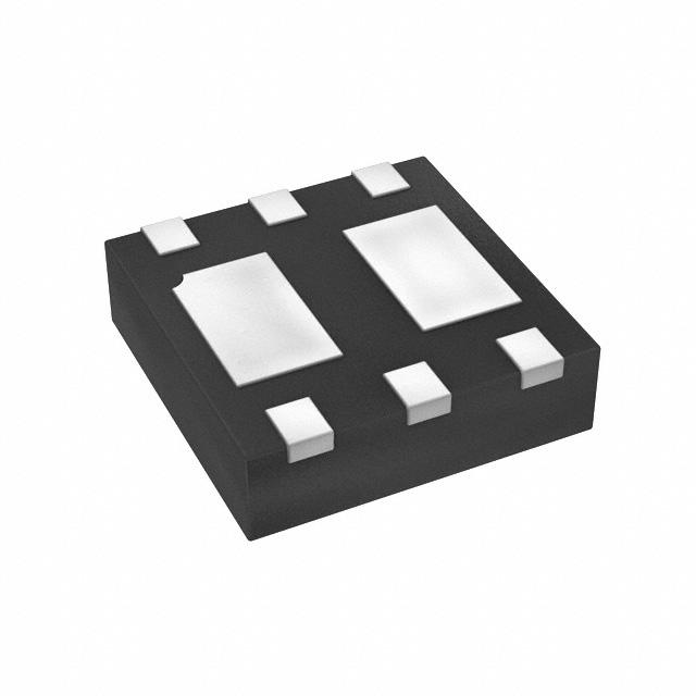
The DMP1046UFDB-7 is a dual P-channel enhancement mode MOSFET manufactured by Diodes Incorporated. It features a U-DFN2020-6 (Type B) surface-mount package with a maximum height of 0.6mm. The device provides a drain-source voltage rating of -12V and a continuous drain current of -3.8A at +25°C. Key electrical parameters include an on-resistance of 61mΩ at VGS = -4.5V, a gate threshold voltage of up to -1V, and a total power dissipation of 1.4W. The component operates within a junction temperature range of -55°C to +150°C.
Verify the specific ordering suffix '-7' corresponds to the 3,000 units per tape and reel packaging format as documented in the manufacturer's ordering information. Confirm that the U-DFN2020-6 (Type B) case material meets the required UL flammability classification rating of 94V-0 for the intended application environment.
Select this component when a compact dual P-channel solution is required for portable power adaptors or load switching circuits. Ensure the design accommodates the specified -12V drain-source voltage limit and verify that the thermal resistance characteristics align with the expected steady-state power dissipation requirements of the system.
This part belongs to the DMP1046UFDB series of dual P-channel enhancement mode MOSFETs from Diodes Incorporated. The product line is engineered to minimize on-state resistance while maintaining superior switching performance. The specific model utilizes a molded plastic case with nickel-palladium-gold terminal finish over a copper leadframe.
The datasheet lists DMP1046UFDB-13 as an alternative packaging option for the same device type. No other direct substitute part numbers are explicitly confirmed in the provided documentation.
The maximum height of the U-DFN2020-6 (Type B) package is 0.6mm.
For automotive applications requiring AEC-Q100/101/200 qualification and IATF 16949 manufacturing, customers must contact Diodes Incorporated directly.
The gate threshold voltage has a maximum value of -1V when tested at VDS = VGS and ID = -250μA.
 DMP1046UFDB-7

The activity of extra discounts on wholesale prices is in full swing…
Please fill in your contact information and we will send you the latest wholesale price list.