 ChipApex | Global Electronic Components Supplier

SEARCH
Search Product
Search Post
— IC芯片 | 连接器 | 传感器 | 被动器件 —
Search productSearch post
— IC芯片 | 连接器 | 传感器 | 被动器件 —
Consult the customer manager about the wholesale price.
consultation hotline:86-132-6715-2157
email:[email protected]
Contact the product manager for consultation. One-stop consultation is available.
Do you want a lower wholesale price? Please send us your inquiry and we will reply immediately.
The DMP2004DMK-7 is a dual P-channel enhancement mode MOSFET in an SOT26 package. It features a drain-source voltage of -20 V and a continuous drain current of -550 mA at +25°C. The device has a maximum power dissipation of 500 mW and operates within a temperature range of -55°C to +150°C. Key electrical parameters include a gate threshold voltage of -1.0 V (max) at -250µA, an input capacitance of 175 pF, and a static on-resistance ranging from 0.7Ω to 2.0Ω depending on the gate-source voltage and drain current conditions.
Verify the specific ordering suffix matches the required packaging format, as the standard designation indicates tape and reel quantities. Confirm that the component meets the necessary environmental compliance standards for your region, specifically checking for halogen and antimony-free status if required by your manufacturing specifications. Ensure the supplier provides traceable documentation for the date code and lot number to maintain quality control records.
Select this component when a compact dual-channel solution is needed for low-voltage P-channel switching applications. The SOT26 package offers space efficiency compared to discrete single transistors. Consider the thermal resistance and power dissipation limits relative to your PCB layout and ambient operating conditions. Verify that the gate drive voltage levels are compatible with the specified threshold voltage characteristics for reliable switching performance.
This part belongs to Diodes Incorporated's DMP series of dual P-channel MOSFETs designed for surface-mount applications. The SOT26 package houses two independent P-channel devices in a single footprint, providing a compact alternative to using two separate SOT23-3 packages. This integration simplifies board layout and reduces overall component count in multi-channel power management designs.
Direct replacements must match the SOT26 package and dual P-channel configuration. Verify that substitute parts meet or exceed the -20V drain-source voltage rating and -550mA continuous current capability. Check that the replacement device also holds AEC-Q101 qualification if used in automotive contexts. Ensure pinout compatibility and similar on-resistance values to maintain circuit performance.
The absolute maximum rating for the gate-source voltage (VGSS) is ±8 V.
Yes, the device is qualified to AEC-Q101 standards for high reliability in automotive environments.
The static drain-source on-resistance decreases as the magnitude of the gate-source voltage increases, ranging from 2.0Ω at -1.8V to 0.7Ω at -4.5V under specific test currents.
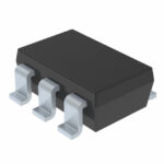 DMP2004DMK-7

The activity of extra discounts on wholesale prices is in full swing…
Please fill in your contact information and we will send you the latest wholesale price list.





