ChipApex | Global Electronic Components Supplier

SEARCH
Search Product
Search Post
— IC芯片 | 连接器 | 传感器 | 被动器件 —
Search productSearch post
— IC芯片 | 连接器 | 传感器 | 被动器件 —
Consult the customer manager about the wholesale price.
consultation hotline:86-132-6715-2157
email:[email protected]
Contact the product manager for consultation. One-stop consultation is available.
Do you want a lower wholesale price? Please send us your inquiry and we will reply immediately.
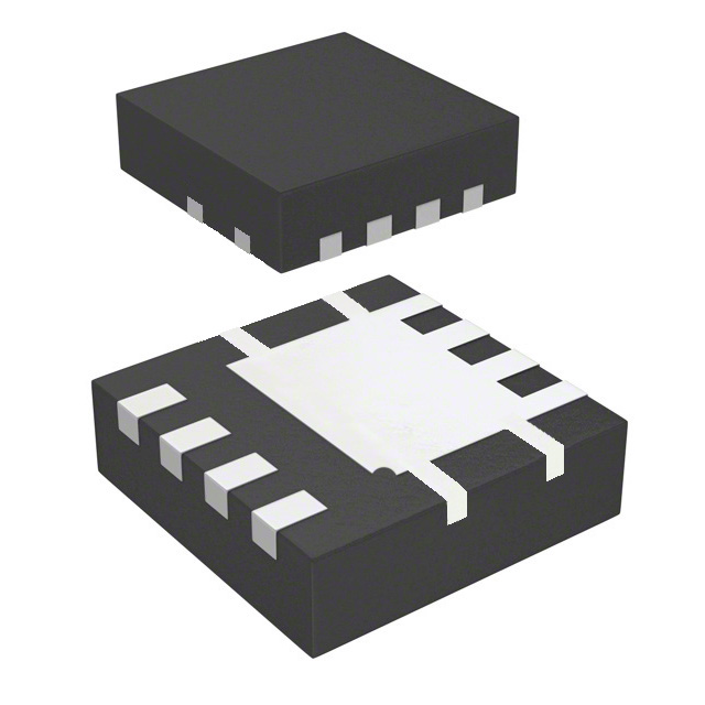
The DMP2010UFV-7 is a 20V P-channel enhancement mode MOSFET from Diodes Incorporated, housed in a PowerDI3333-8 (Type UX) package. It features a maximum drain-source voltage of -20V and a gate-source voltage rating of ±10V. The device offers a typical static drain-source on-resistance of 7.5mΩ at VGS = -4.5V, with a maximum of 9.5mΩ under the same conditions. At VGS = -2.5V, the RDS(ON) is typically 12.5mΩ. Continuous drain current reaches -50A at TC = +25°C, reducing to -40A at TC = +70°C. Pulsed drain current is rated at -80A. Thermal resistance junction-to-ambient is 122°C/W on FR-4 with minimum pads, or 62°C/W with thermal bias.
Verify the specific ordering suffix when purchasing. The DMP2010UFV-7 variant comes in a tape and reel packaging format containing 2000 units per reel. Confirm that the component matches the PowerDI3333-8 case style and Type UX designation. Ensure compatibility with standard surface mount assembly processes. Check for moisture sensitivity level 1 compliance as per J-STD-020 standards before storage and handling.
Select this component for applications requiring low on-resistance in a compact footprint. The PowerDI3333-8 package provides thermal efficiency suitable for dense PCB layouts. Consider the gate threshold voltage characteristics for logic level driving requirements. Evaluate thermal dissipation capabilities based on the specific board copper area and ambient temperature conditions. Ensure the voltage ratings align with the system's maximum operating voltages.
This part belongs to the DMP series of P-channel MOSFETs from Diodes Incorporated. It utilizes the PowerDI proprietary surface mount package technology. The device is engineered for general purpose power switching applications where space constraints and thermal performance are critical factors. It serves as a direct replacement for larger through-hole or standard surface mount packages in modern portable electronics.
Check datasheets for alternative P-channel MOSFETs with similar -20V ratings and comparable RDS(ON) values. Verify pinout compatibility if substituting in existing designs. Ensure the replacement package fits within the mechanical constraints of the original layout. Confirm that thermal resistance characteristics meet the system's cooling requirements.
The maximum continuous drain current decreases to -40A when the case temperature is maintained at +70°C.
The typical RDS(ON) is 7.5mΩ at VGS = -4.5V and increases to a typical value of 12.5mΩ at VGS = -2.5V.
 DMP2010UFV-7

The activity of extra discounts on wholesale prices is in full swing…
Please fill in your contact information and we will send you the latest wholesale price list.