ChipApex | Global Electronic Components Supplier

SEARCH
Search Product
Search Post
— IC芯片 | 连接器 | 传感器 | 被动器件 —
Search productSearch post
— IC芯片 | 连接器 | 传感器 | 被动器件 —
Consult the customer manager about the wholesale price.
consultation hotline:86-132-6715-2157
email:[email protected]
Contact the product manager for consultation. One-stop consultation is available.
Do you want a lower wholesale price? Please send us your inquiry and we will reply immediately.
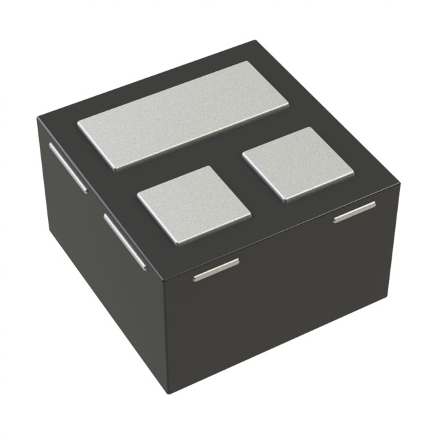
The DMP22D3UFZ-7B is a P-channel enhancement mode MOSFET from Diodes Incorporated, housed in an X2-DFN0606-3 package. It features a drain-source voltage (V_DSS) of -20 V and a maximum gate-source voltage (V_GS) of ±8 V. The device offers low on-resistance, with R_DS(ON) values ranging from 1.4 Ω at V_GS = -4.5 V to 5.0 Ω at V_GS = -1.5 V. Continuous drain current (I_D) reaches -0.39 A at +25°C. Key electrical parameters include a gate threshold voltage (V_GS(TH)) max of -1.0 V, total gate charge (Q_g) of 0.3 nC, and input capacitance (C_iss) of 17 pF. Operating temperature ranges from -55°C to +150°C.
Verify the specific ordering suffix '-7B' corresponds to the 10k Tape & Reel packaging configuration as documented in the manufacturer's ordering information. Confirm that the component meets RoHS 3 compliance and Halogen/Antimony-free requirements if environmental standards are critical to the design. Ensure the selected part number matches the exact electrical characteristics defined in the datasheet.
Select this component when space constraints require the X2-DFN0606-3 package and low on-resistance is prioritized for efficiency. Consider the -20 V rating and -0.39 A continuous current capability against load requirements. Evaluate the low gate threshold voltage (-1.0 V max) compatibility with available drive voltages. Verify thermal dissipation needs against the specified junction-to-ambient thermal resistance.
This component belongs to the DMP22 series of P-channel MOSFETs designed by Diodes Incorporated. These devices utilize silicon technology and are intended for surface-mount applications requiring small footprints. The series focuses on balancing low static losses with fast dynamic switching capabilities suitable for modern portable and battery-powered electronics.
Consult official Diodes Incorporated documentation or authorized distributors for confirmed substitute part numbers. Do not assume cross-compatibility based solely on package type or general specifications without verifying electrical limits and pin configurations.
The absolute maximum rating for Gate-Source Voltage (V_GS) is ±8 V.
R_DS(ON) increases as the magnitude of the gate-source voltage decreases. It is 1.4 Ω max at -4.5 V and rises to 5.0 Ω max at -1.5 V.
 DMP22D3UFZ-7B

The activity of extra discounts on wholesale prices is in full swing…
Please fill in your contact information and we will send you the latest wholesale price list.