ChipApex | Global Electronic Components Supplier

SEARCH
Search Product
Search Post
— IC芯片 | 连接器 | 传感器 | 被动器件 —
Search productSearch post
— IC芯片 | 连接器 | 传感器 | 被动器件 —
Consult the customer manager about the wholesale price.
consultation hotline:86-132-6715-2157
email:[email protected]
Contact the product manager for consultation. One-stop consultation is available.
Do you want a lower wholesale price? Please send us your inquiry and we will reply immediately.
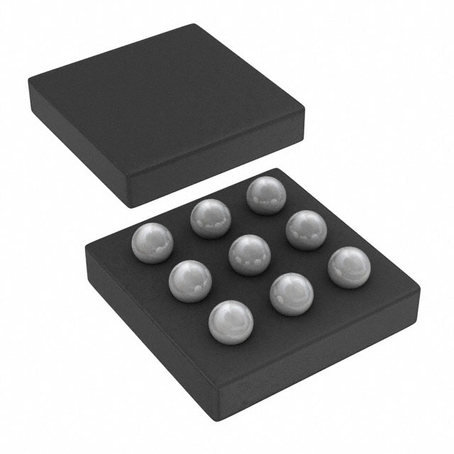
The DMP2540UCB9-7 is a P-channel enhancement mode MOSFET from Diodes Incorporated, utilizing LD-MOS technology. It features a -25V drain-source voltage (VDSS) and a typical on-resistance of 33mΩ at VGS = -4.5V. The device supports a continuous drain current of -5.2A at +25°C and offers ultra-fast switching with a total gate charge of 4.8nC. Packaged in the U-WLB1515-9 CSP footprint measuring 1.5mm x 1.5mm with a height of 0.62mm, it operates within a temperature range of -55°C to +150°C.
Verify component authenticity by checking the marking code against the manufacturer's date code key. Confirm compliance with RoHS directives and ensure the package matches the specified U-WLB1515-9 dimensions. Validate that the ordering suffix corresponds to the required tape and reel packaging quantity before finalizing procurement orders.
Select this component when low profile and minimal on-state resistance are critical for power efficiency. Ensure the application requires a -25V rating and can accommodate the specific thermal characteristics of the U-WLB1515-9 package. Verify that the gate drive voltage aligns with the low threshold requirements for optimal switching performance.
This part belongs to the DMP series of P-channel MOSFETs designed for high-efficiency power management. It represents an advancement in LD-MOS technology, focusing on reducing the figure of merit between on-resistance and gate charge. The compact CSP package allows for dense PCB layouts in portable and automotive electronics.
Consult official substitution lists for verified alternatives. Cross-reference pin configurations and electrical parameters carefully to ensure compatibility without modifying existing circuit designs or thermal management strategies.
The device supports a pulsed drain current of -30A with a pulse duration of 10μs and a duty cycle of 1% or less.
The static drain-source on-resistance increases as the gate-source voltage decreases, measured at 33mΩ at -4.5V, 42mΩ at -2.5V, and 52mΩ at -1.8V.
 DMP2540UCB9-7

The activity of extra discounts on wholesale prices is in full swing…
Please fill in your contact information and we will send you the latest wholesale price list.