 ChipApex | Global Electronic Components Supplier

SEARCH
Search Product
Search Post
— IC芯片 | 连接器 | 传感器 | 被动器件 —
Search productSearch post
— IC芯片 | 连接器 | 传感器 | 被动器件 —
Consult the customer manager about the wholesale price.
consultation hotline:86-132-6715-2157
email:[email protected]
Contact the product manager for consultation. One-stop consultation is available.
Do you want a lower wholesale price? Please send us your inquiry and we will reply immediately.
The DMP2900UDW-13 is a dual p-channel enhancement mode MOSFET manufactured by Diodes Incorporated. It integrates two independent P-channel MOSFETs within a single SOT363 surface-mount package. The device features a drain-source voltage (BVDSS) of -20V and a maximum continuous drain current of -0.63A at +25°C. Static drain-source on-resistance (RDS(ON)) is specified as 0.75Ω max at VGS = -4.5V and 1.05Ω max at VGS = -2.5V. Total gate charge is typically 0.7nC, with turn-on delay time at 16ns. Operating temperature range spans from -55°C to +150°C.
Verify the specific ordering suffix '-13' corresponds to the 10,000-unit tape and reel packaging format. Confirm that the component meets all applicable environmental directives, including RoHS 3 compliance and halogen-free status, as defined by the manufacturer's quality definitions. Ensure the procurement channel is authorized to guarantee product authenticity and traceability.
Select this component when space constraints require dual switch functionality within an ultra-small SOT363 footprint. Evaluate thermal management requirements against the junction-to-ambient thermal resistance values provided in the datasheet. Verify that the required gate drive voltage aligns with the specified RDS(ON) characteristics to ensure optimal efficiency in power management applications.
This part belongs to Diodes Incorporated's advanced generation MOSFET portfolio designed for high-efficiency power management. The DMP2900UDW series specifically targets applications requiring minimized on-state resistance without compromising switching speed. It serves as a compact solution for replacing discrete dual-MOSFET arrangements in portable and battery-powered electronics.
Consult official cross-reference tools or contact Diodes Incorporated directly for verified substitute part numbers. Do not assume functional equivalence based solely on package type or generic specifications.
The device includes an integrated gate protection diode to provide electrostatic discharge (ESD) protection.
The static drain-source on-resistance decreases as the magnitude of the gate-source voltage increases, with lower resistance values achieved at VGS = -4.5V compared to -2.5V or -1.8V.
For automotive applications requiring specific change control or AEC-Q qualification, customers must contact Diodes Incorporated or their local representative directly.
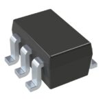 DMP2900UDW-13

The activity of extra discounts on wholesale prices is in full swing…
Please fill in your contact information and we will send you the latest wholesale price list.





