 ChipApex | Global Electronic Components Supplier
SEARCH
Search Product
Search Post
— IC芯片 | 连接器 | 传感器 | 被动器件 —
Search productSearch post
— IC芯片 | 连接器 | 传感器 | 被动器件 —
Consult the customer manager about the wholesale price.
consultation hotline:86-132-6715-2157
email:[email protected]
Contact the product manager for consultation. One-stop consultation is available.
Do you want a lower wholesale price? Please send us your inquiry and we will reply immediately.
The DMP3098LQ-7 is a single P-channel enhancement mode MOSFET manufactured by Diodes Incorporated. It features a maximum drain-source voltage (V(BR)DSS) of -30V and a continuous drain current (ID) of -3.8A at +25°C. The device exhibits a maximum static drain-source on-resistance (RDS(ON)) of 70mΩ at VGS = -10V and 120mΩ at VGS = -4.5V. Total gate charge (Qg) is typically 4.0nC at VGS = -4.5V. Operating temperature range spans from -55°C to +150°C, with total power dissipation rated at 1.08W.
Verify the specific ordering suffix '-7' corresponds to the tape and reel packaging configuration containing 3,000 units per reel. Confirm that the component meets the required AEC-Q101 qualification standards if intended for automotive use. Ensure the SOT-23 package dimensions align with the target PCB footprint layout requirements.
Select this component when a low on-resistance P-channel MOSFET is required for efficient power management circuits. The device offers fast switching speeds suitable for boost switch and load switch topologies. Consider the thermal characteristics and power dissipation limits relative to the ambient operating conditions and PCB copper pad area available for heat sinking.
This part belongs to the DMP3098 series of P-channel enhancement mode MOSFETs produced by Diodes Incorporated. The series is engineered to provide low on-state resistance combined with fast switching capabilities. The DMP3098LQ variant specifically utilizes an SOT-23 case outline and holds AEC-Q101 qualification for automotive reliability standards.
Check datasheets for alternative P-channel MOSFETs in the SOT-23 package with comparable V(BR)DSS and RDS(ON) specifications. Verify pinout compatibility and thermal resistance values before substitution. Ensure any replacement part also meets AEC-Q101 requirements if used in automotive contexts.
The maximum drain-source breakdown voltage (V(BR)DSS) is -30V.
Yes, the DMP3098LQ is qualified to AEC-Q101 standards for high reliability automotive applications.
The typical total gate charge (Qg) is 4.0nC when tested at VDS = -15V, VGS = -4.5V, and ID = -3.8A.
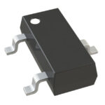 DMP3098LQ-7
The activity of extra discounts on wholesale prices is in full swing…
Please fill in your contact information and we will send you the latest wholesale price list.





