ChipApex | Global Electronic Components Supplier

SEARCH
Search Product
Search Post
— IC芯片 | 连接器 | 传感器 | 被动器件 —
Search productSearch post
— IC芯片 | 连接器 | 传感器 | 被动器件 —
Consult the customer manager about the wholesale price.
consultation hotline:86-132-6715-2157
email:[email protected]
Contact the product manager for consultation. One-stop consultation is available.
Do you want a lower wholesale price? Please send us your inquiry and we will reply immediately.
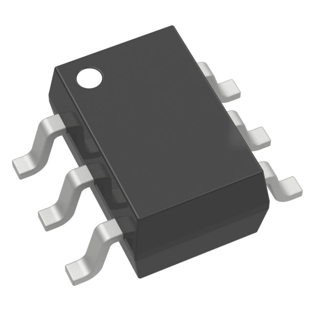
The DMP3164LVT-13 is a dual P-channel enhancement mode MOSFET in a TSOT26 package. It features a -30V drain-source voltage rating and operates within a -55°C to +150°C junction temperature range. At VGS = -10V, the on-resistance is typically 95mΩ with a continuous current of -2.8A. At VGS = -4.5V, resistance is 140mΩ with -2.3A current. The device includes low input capacitance (324pF) and gate charge values of 4.4nC at -4.5V and 8.6nC at -10V.
Verify the specific ordering suffix matches the required tape and reel quantity. Confirm that the component meets all applicable environmental directives relevant to the target market. Ensure the datasheet revision aligns with the manufacturing date code on the received units.
Select this component when a dual P-channel solution is required in a small footprint. Evaluate the thermal resistance limits against the expected ambient conditions. Verify that the gate drive voltage supports the desired on-resistance level for the specific application load.
This part belongs to Diodes Incorporated's generation of low RDS(ON) MOSFETs designed for high efficiency applications. It utilizes a TSOT26 case material with a molded plastic green molding compound. The terminals are finished with matte tin annealed over a copper leadframe.
Check pinout compatibility and electrical ratings before substituting. No public confirmed substitute part numbers are available in the source documentation.
The absolute maximum rating for gate-source voltage is ±12 V.
On-resistance decreases as the magnitude of the gate-source voltage increases, dropping from a typical 140mΩ at -4.5V to 95mΩ at -10V.
Yes, the operating and storage temperature range extends up to +150°C.
 DMP3164LVT-13

The activity of extra discounts on wholesale prices is in full swing…
Please fill in your contact information and we will send you the latest wholesale price list.