 ChipApex | Global Electronic Components Supplier

SEARCH
Search Product
Search Post
— IC芯片 | 连接器 | 传感器 | 被动器件 —
Search productSearch post
— IC芯片 | 连接器 | 传感器 | 被动器件 —
Consult the customer manager about the wholesale price.
consultation hotline:86-132-6715-2157
email:[email protected]
Contact the product manager for consultation. One-stop consultation is available.
Do you want a lower wholesale price? Please send us your inquiry and we will reply immediately.
The DMP31D7LDW-7 is a dual P-channel enhancement mode MOSFET in an SOT363 package. It features a drain-source voltage (V_DSS) of -30 V and a maximum continuous drain current (I_D) of -0.55 A at +25°C. The on-resistance (R_DS(ON)) is 0.9 Ω max at V_GS = -10 V and 1.7 Ω max at V_GS = -4.5 V. Total power dissipation is 0.29 W at +25°C with a thermal resistance (R_θJA) of 433 °C/W. Operating temperature range is -55°C to +150°C.
Verify the specific ordering suffix (-7 or -13) against your required tape and reel quantity. Confirm that the standard commercial version meets your application requirements, as automotive-compliant variants are available under separate datasheets. Ensure proper handling for ESD-sensitive components during assembly.
Select this component for applications requiring dual P-channel switching in a compact SOT363 footprint. Evaluate the R_DS(ON) values at your specific gate drive voltages (-4.5 V or -10 V) to ensure acceptable conduction losses. Consider the thermal resistance limits when designing heat dissipation strategies for steady-state operations.
This device belongs to Diodes Incorporated's DMP series of dual P-channel enhancement mode MOSFETs. It is designed to minimize on-state resistance while maintaining superior switching performance. The product is totally lead-free, fully RoHS compliant, and halogen and antimony free.
An automotive-compliant part is available under a separate datasheet: DMP31D7LDWQ.
The maximum continuous drain current is -0.55 A at an ambient temperature of +25°C.
The standard DMP31D7LDW-7 is not explicitly stated as automotive-grade. An automotive-compliant version, DMP31D7LDWQ, is available under a separate datasheet.
The typical total gate charge is 0.36 nC at V_GS = -4.5 V and 0.8 nC at V_GS = -10 V.
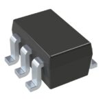 DMP31D7LDW-7

The activity of extra discounts on wholesale prices is in full swing…
Please fill in your contact information and we will send you the latest wholesale price list.





