 ChipApex | Global Electronic Components Supplier

SEARCH
Search Product
Search Post
— IC芯片 | 连接器 | 传感器 | 被动器件 —
Search productSearch post
— IC芯片 | 连接器 | 传感器 | 被动器件 —
Consult the customer manager about the wholesale price.
consultation hotline:86-132-6715-2157
email:[email protected]
Contact the product manager for consultation. One-stop consultation is available.
Do you want a lower wholesale price? Please send us your inquiry and we will reply immediately.
The DMP6050SSD-13 is a dual P-channel enhancement mode MOSFET manufactured by Diodes Incorporated. It features a -60V drain-source voltage rating and a maximum continuous drain current of -4.8A at +25°C ambient temperature. The device exhibits a low on-state resistance of 55mΩ at VGS = -10V and 70mΩ at VGS = -4.5V. Packaged in an SO-8 surface mount case, it supports a total power dissipation of 1.2W at +25°C with a thermal resistance junction-to-ambient of 104°C/W.
Verify the specific ordering suffix '-13' corresponds to the 2500-unit tape and reel packaging format. Confirm that the component meets the required environmental standards, specifically the halogen-free and antimony-free 'Green' device definition provided by the manufacturer. Ensure compatibility with standard SO-8 pad layouts for proper solderability.
Select this component for applications requiring a dual P-channel MOSFET with a -60V breakdown voltage. Consider the thermal performance characteristics, including the 104°C/W junction-to-ambient resistance, when designing heat dissipation strategies. Evaluate the gate threshold voltage range to ensure compatibility with the intended logic drive levels for optimal switching performance.
This part belongs to the DMP series of dual P-channel enhancement mode MOSFETs from Diodes Incorporated. It is designed to offer superior switching performance while maintaining low on-state resistance. The device utilizes an SO-8 package suitable for surface mount technology, providing a compact solution for space-constrained power management designs.
Consult official manufacturer documentation for verified equivalent parts. Cross-referencing should focus on matching electrical parameters such as voltage ratings, current capabilities, and package dimensions to ensure functional compatibility without compromising circuit integrity.
The maximum continuous drain current (ID) at TA = +25°C is -4.8A.
Yes, the device is totally lead-free and fully RoHS compliant, as well as being halogen and antimony free.
The total gate charge (Qg) is typically 24nC when tested at VGS = -10V, VDS = -30V, and ID = -5A.
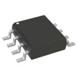 DMP6050SSD-13

The activity of extra discounts on wholesale prices is in full swing…
Please fill in your contact information and we will send you the latest wholesale price list.





