 ChipApex | Global Electronic Components Supplier

SEARCH
Search Product
Search Post
— IC芯片 | 连接器 | 传感器 | 被动器件 —
Search productSearch post
— IC芯片 | 连接器 | 传感器 | 被动器件 —
Consult the customer manager about the wholesale price.
consultation hotline:86-132-6715-2157
email:[email protected]
Contact the product manager for consultation. One-stop consultation is available.
Do you want a lower wholesale price? Please send us your inquiry and we will reply immediately.
The DMP6051SSD-13 is a dual P-channel enhancement mode MOSFET manufactured by Diodes Incorporated. It features a -60V drain-source voltage rating and a maximum continuous drain current of -4.3A at +25°C. The device offers a low on-resistance of 60mΩ at VGS = -10V and 80mΩ at VGS = -4.5V. Packaged in an SO-8 surface-mount format, it supports a total power dissipation of 1.4W to 1.6W depending on board layout. The component operates within a junction temperature range of -55°C to +150°C.
Verify the specific ordering suffix '-13' corresponds to the Tape & Reel packaging quantity of 2,500 units as defined in the manufacturer's documentation. Confirm that the required operating conditions align with the specified thermal resistance values for the chosen PCB copper area. Ensure compliance with RoHS 3 and Halogen-free requirements if mandated by the end-use environment.
Select this component when a dual P-channel topology is required for synchronous rectification or high-side switching. Evaluate the gate threshold voltage characteristics against the available drive voltage levels to ensure full enhancement. Consider the thermal resistance parameters relative to the expected ambient temperature and duty cycle to maintain junction temperatures within safe operating limits.
This part belongs to the DMP series of dual P-channel MOSFETs from Diodes Incorporated. It utilizes an SO-8 package constructed with a molded plastic compound classified as UL 94V-0. The terminals feature a tin finish annealed over a copper leadframe, ensuring solderability per MIL-STD-208 standards.
The datasheet references the Q-suffix variant for automotive applications requiring AEC-Q qualification and PPAP capability. Verify pinout compatibility and electrical parameter equivalence before substituting with other dual P-channel MOSFETs.
The maximum pulsed drain current is -30A, measured with a 10μs pulse duration and a 1% duty cycle.
Yes, the device has a rated avalanche energy of 37.5 mJ with an inductance of 0.1mH.
The total gate charge is typically 36 nC when tested at VDS = -30V and ID = -5A.
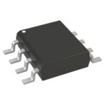 DMP6051SSD-13

The activity of extra discounts on wholesale prices is in full swing…
Please fill in your contact information and we will send you the latest wholesale price list.





