ChipApex | Global Electronic Components Supplier
SEARCH
Search Product
Search Post
— IC芯片 | 连接器 | 传感器 | 被动器件 —
Search productSearch post
— IC芯片 | 连接器 | 传感器 | 被动器件 —
Consult the customer manager about the wholesale price.
consultation hotline:86-132-6715-2157
email:[email protected]
Contact the product manager for consultation. One-stop consultation is available.
Do you want a lower wholesale price? Please send us your inquiry and we will reply immediately.
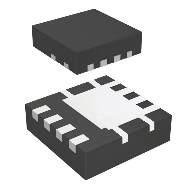
The DMS3012SFG-7 is a 30V N-channel enhancement mode MOSFET with an integrated Schottky diode, manufactured by Diodes Incorporated. It utilizes the DIOFET patented process to monolithically integrate components on a single die. The device features a maximum drain-source voltage of 30V and continuous drain currents ranging from 9.5A to 16.0A depending on thermal conditions. On-resistance is specified at 10mΩ at VGS=10V and 15mΩ at VGS=4.5V. It operates within a temperature range of -55°C to +150°C and is housed in a PowerDI3333-8 package.
Verify component authenticity through authorized channels as counterfeit risks exist. Confirm RoHS compliance status and lead-free specifications against current regulatory requirements. Check datasheet revision history for any parameter updates. Ensure storage conditions meet moisture sensitivity level standards prior to soldering. Validate package dimensions against PCB footprint requirements.
Evaluate thermal performance based on specific PCB copper area and ambient temperature conditions. Compare on-resistance values at intended gate drive voltages to ensure efficiency targets are met. Consider the integrated Schottky diode characteristics for synchronous rectification applications. Assess package compatibility with automated assembly processes and reflow soldering profiles.
This component belongs to the DMS30 series of asymmetric dual N-channel enhancement mode MOSFETs produced by Diodes Incorporated. The series leverages proprietary DIOFET technology to combine power switching and freewheeling functions. The PowerDI3333-8 package provides a compact solution for space-constrained designs requiring high reliability and low thermal resistance.
The datasheet explicitly states 'NOT RECOMMENDED FOR NEW DESIGN - NO ALTERNATE PART'. No official substitute part numbers are provided by the manufacturer. Design modifications may be required if sourcing this component for new production runs.
The integrated Schottky diode reduces losses due to body diode conduction and lowers reverse recovery charge (Qrr), which minimizes body diode switching losses.
It provides a low gate capacitance (Qg/Qgs) ratio, which reduces the risk of shoot-through or cross-conduction currents during high-frequency switching.
 DMS3012SFG-7
The activity of extra discounts on wholesale prices is in full swing…
Please fill in your contact information and we will send you the latest wholesale price list.