ChipApex | Global Electronic Components Supplier

SEARCH
Search Product
Search Post
— IC芯片 | 连接器 | 传感器 | 被动器件 —
Search productSearch post
— IC芯片 | 连接器 | 传感器 | 被动器件 —
Consult the customer manager about the wholesale price.
consultation hotline:86-132-6715-2157
email:[email protected]
Contact the product manager for consultation. One-stop consultation is available.
Do you want a lower wholesale price? Please send us your inquiry and we will reply immediately.
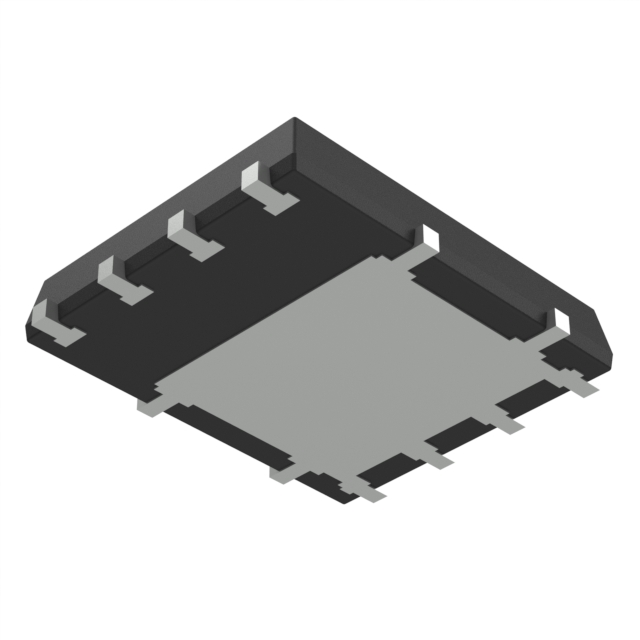
The DMTH6010LPD-13 is a dual N-channel enhancement mode MOSFET from Diodes Incorporated, housed in a PowerDI5060-8 surface-mount package. It features a drain-source voltage (V_DSS) of 60V and a maximum on-resistance (R_DS(ON)) of 11mΩ at V_GS = 10V and I_D = 20A. The device supports a continuous drain current of 47.6A at case temperatures of +25°C and operates within a junction temperature range of -55°C to +175°C. Total power dissipation reaches 2.8W at ambient temperatures of +25°C.
Verify the specific package variant against the datasheet before ordering, as the DMTH6010LPD-13 designation covers both Type C and Type UXD configurations within the PowerDI5060-8 footprint. Confirm that the required packing quantity aligns with the standard 2,500 units per tape and reel carrier specified by the manufacturer.
Select this component when a dual N-channel configuration is required in a compact surface-mount form factor. Ensure the application's thermal design accommodates the specified R_θJA of 53°C/W for steady-state operations on FR-4 substrates. Verify that gate drive voltages meet the thresholds for the desired R_DS(ON) levels.
This part belongs to the DMTH6010 series of automotive-grade MOSFETs designed by Diodes Incorporated. It utilizes the PowerDI® trademarked packaging technology to provide robust thermal performance and low profile. The series is intended for applications requiring high conversion efficiency and reliability in demanding electronic environments.
For automotive applications requiring specific change control or AEC-Q100/101 qualification, consult the separate datasheet for the DMTH6010LPDQ variant. Direct cross-referencing with other manufacturers requires careful verification of pinout compatibility and thermal characteristics due to the proprietary PowerDI package geometry.
The maximum pulsed drain current (I_DM) is rated at 170A, based on a 10µs pulse duration with a duty cycle of 1%.
Yes, the device undergoes 100% Unclamped Inductive Switching (UIS) testing in production to ensure reliability under such conditions.
At V_GS = 10V, V_DS = 30V, and I_D = 20A, the total gate charge (Q_g) is typically 40.2nC, with a gate-source charge (Q_gs) of 5.9nC and gate-drain charge (Q_gd) of 9.3nC.
 DMTH6010LPD-13

The activity of extra discounts on wholesale prices is in full swing…
Please fill in your contact information and we will send you the latest wholesale price list.